- 您现在的位置:买卖IC网 > PDF目录11767 > AD6620ASZ-REEL (Analog Devices Inc)IC DGTL RCVR DUAL 67MSPS 80-PQFP PDF资料下载
参数资料
| 型号: | AD6620ASZ-REEL |
| 厂商: | Analog Devices Inc |
| 文件页数: | 14/44页 |
| 文件大小: | 0K |
| 描述: | IC DGTL RCVR DUAL 67MSPS 80-PQFP |
| 标准包装: | 500 |
| 接口: | 并行/串行 |
| 电源电压: | 3 V ~ 3.6 V |
| 封装/外壳: | 80-BQFP |
| 供应商设备封装: | 80-PQFP(14x14) |
| 包装: | 带卷 (TR) |
| 安装类型: | 表面贴装 |
第1页第2页第3页第4页第5页第6页第7页第8页第9页第10页第11页第12页第13页当前第14页第15页第16页第17页第18页第19页第20页第21页第22页第23页第24页第25页第26页第27页第28页第29页第30页第31页第32页第33页第34页第35页第36页第37页第38页第39页第40页第41页第42页第43页第44页
AD6620
–21–
REV. A
The frequency of the SYNC_NCO pulses, and therefore the
accuracy of the synchronization, is determined by the value of
the NCO Sync Control Register at address 302 hex. The value
in this register is the SYNC_MASK and is interpreted as a
32-bit unsigned integer. This value controls the window around
the zero crossing of the NCO output sine wave in which the
NCO will output a SYNC_NCO pulse as a master. As a slave,
the value in this register will determine the number of MSBs
of the output sine wave that are synchronized with the master.
The Master and all slaves should use the same SYNC_MASK
word. This value should almost always be written as all 1s
(FFFFFFFF hex).
Effects of A/B Input on the NCO
If the AD6620 is run in Single Channel Real mode using frac-
tional rate input timing, the A/B input is used to enable the
NCO advancement. If the A/B line is held high longer than one
clock period, the NCO will advance for each rising edge of the
CLK while A/B is high. This is not normally the desired result
and thus A/B must be taken low after the first CLK period to
prevent anomalous NCO results. See additional details under
Fractional Rate Timing.
Phase Continuous Tuning with the AD6620
For synchronization purposes, the AD6620 NCO phase is reset
each time the NCO frequency register is either written to or
read from. This is accomplished by forcing an NCO Sync to
occur. Normally, phase-continuous tuning is required on the
transmit path to control spectral leakage. On the receive path
this in not usually a constraint. However, if phase-continuous
tuning is required with the AD6620, it can be accomplished by
configuring the AD6620 as a Sync Slave. In this manner, no
internal NCO sync is generated when the NCO frequency regis-
ter is written to. If multiple AD6620s are synchronized together,
a common external sync pulse can be used to lock each of the
receivers together at the appropriate point in time. It is also
possible to reconfigure the AD6620 after the NCO frequency
register has been written so that the chip is once again a Sync
Master. The next time the NCO phase cycles through 0 degrees,
the NCO sync is exerted and the chip is again synchronized.
2ND ORDER CASCADED INTEGRATOR COMB FILTER
The CIC2 filter is a fixed-coefficient, decimating filter. It is
constructed as a second order CIC filter whose characteristics
are defined only by the decimation rate chosen. This filter can
process signals at the full rate of the input port (67 MHz) in all
input modes. The output rate of this stage is given by the equa-
tion below.
f
M
SAMP
CIC
2
=
The decimation ratio, MCIC2, is an unsigned integer that may
be between 1 and 16. This stage may be bypassed under certain
conditions by setting, MCIC2 equal to 1. For this to happen the
processing clock rate, fCLK must be two or more times the input
data rate, fSAMP. This is because the I and Q data is processed in
parallel within the CIC2 filter, and the I and Q output data is
then multiplexed through the same data pipe before it enters the
CIC5 filter.
The frequency response of the CIC2 filter is given by the follow-
ing equations.
Hz
z
S
M
CIC
()
–
=×
1
2
1
2
1
2
Hf
Mf
f
S
CIC
SAMP
CIC
()
sin
=×
×
1
2
π
The scale factor, SCIC2 is a programmable unsigned integer
between 0 and 6. This serves as an attenuator that can reduce
the gain of the CIC2 in 6 dB increments. For the best dynamic
range, SCIC2 should be set to the smallest value possible (i.e.,
lowest attenuation) without creating an overflow condition.
This can be safely accomplished using the equation below, where
input_level is the largest fraction of full scale possible at the
input to this AD6620 (normally 1). The CIC2 scale factor is
not ignored when the CIC2 is bypassed.
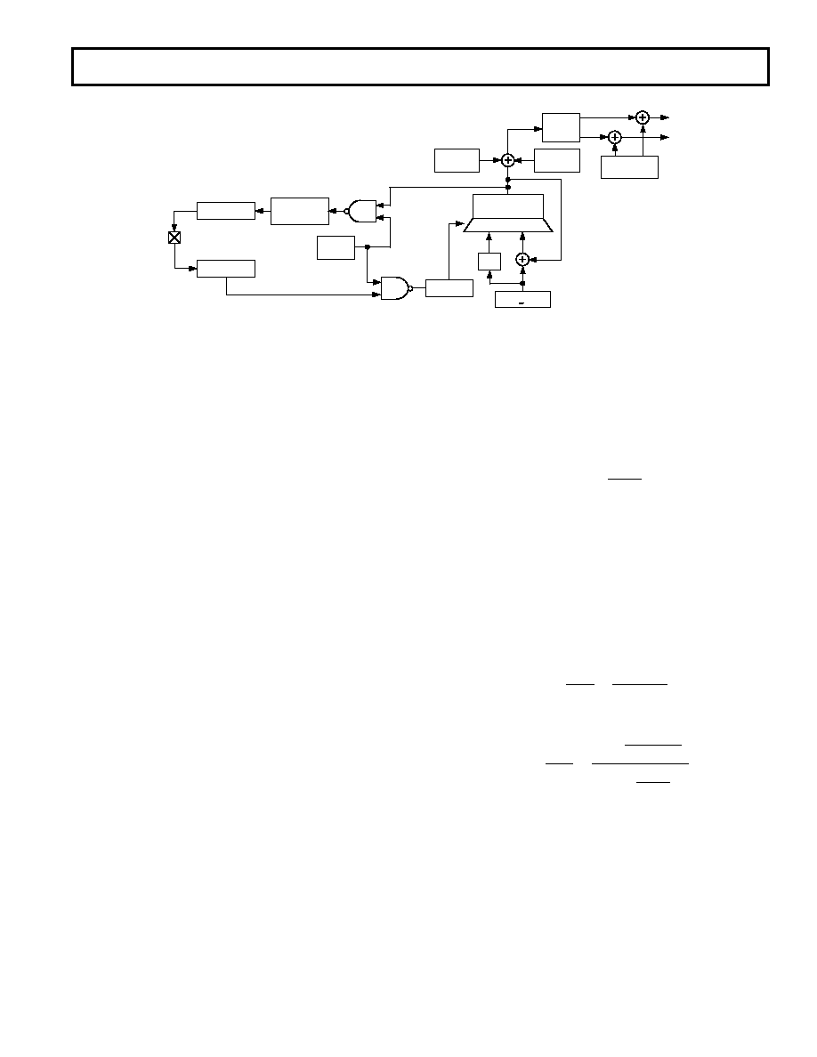
REGISTER
1
MASKED
COUNT = 0?
SYNC
MASK
SYNC_NCO
PIN
1
32
1
0
32
NCO FREQ
AMPLITUDE
DITHER
COS
SIN
PHASE
DITHER
PHASE
OFFSET
PHASE
ACCUMULATOR
X4
REGISTER
Figure 35. NCO Block Diagram
相关PDF资料 |
PDF描述 |
|---|---|
| 6274291-2 | CONN JACK VERT PCB 75 OHM BNC |
| AD7669JNZ | IC I/O PORT 8BIT ANLG 28DIP |
| D38999/24FF11PA | CONN RCPT 11POS JAM NUT W/PINS |
| D38999/20JE26HN | CONN RCPT 26POS WALL MNT W/PINS |
| AD7569KNZ | IC I/O PORT 8BIT ANALOG 24DIP |
相关代理商/技术参数 |
参数描述 |
|---|---|
| AD6620PCB | 制造商:AD 制造商全称:Analog Devices 功能描述:65 MSPS Digital Receive Signal Processor |
| AD6620S | 制造商:AD 制造商全称:Analog Devices 功能描述:65 MSPS Digital Receive Signal Processor |
| AD6620S/PCB | 制造商:Analog Devices 功能描述:DUAL CHANNEL DECIMATING RECEIV 制造商:Analog Devices 功能描述:SGNL PROCESSOR 169CSPBGA - Bulk |
| AD6622 | 制造商:AD 制造商全称:Analog Devices 功能描述:Four-Channel, 75 MSPS Digital Transmit Signal Processor TSP |
| AD6622AS | 制造商:Analog Devices 功能描述:Transmit Signal Processor 128-Pin MQFP 制造商:Rochester Electronics LLC 功能描述:4 CHANNEL 65 MSPS DIGITAL UPCONVERTER - Bulk |
发布紧急采购,3分钟左右您将得到回复。