- 您现在的位置:买卖IC网 > PDF目录11767 > AD6620ASZ-REEL (Analog Devices Inc)IC DGTL RCVR DUAL 67MSPS 80-PQFP PDF资料下载
参数资料
| 型号: | AD6620ASZ-REEL |
| 厂商: | Analog Devices Inc |
| 文件页数: | 8/44页 |
| 文件大小: | 0K |
| 描述: | IC DGTL RCVR DUAL 67MSPS 80-PQFP |
| 标准包装: | 500 |
| 接口: | 并行/串行 |
| 电源电压: | 3 V ~ 3.6 V |
| 封装/外壳: | 80-BQFP |
| 供应商设备封装: | 80-PQFP(14x14) |
| 包装: | 带卷 (TR) |
| 安装类型: | 表面贴装 |
第1页第2页第3页第4页第5页第6页第7页当前第8页第9页第10页第11页第12页第13页第14页第15页第16页第17页第18页第19页第20页第21页第22页第23页第24页第25页第26页第27页第28页第29页第30页第31页第32页第33页第34页第35页第36页第37页第38页第39页第40页第41页第42页第43页第44页
AD6620
–16–
REV. A
The Exponent Offset is used to shift the data right. For example,
Table I shows that with no ExpOff shift, 12 dB of range is
lost when the ADC input is at the largest level. This is undesired
because it lowers the Dynamic Range and SNR of the system
by reducing the signal of interest relative to the quantization
noise floor.
To avoid this automatic attenuation of the full-scale ADC sig-
nal, the Exponent Offset is used to move the largest signal (RSSI =
5) up to the point where there is no downshift. In other words,
once the Exponent Invert bit has been set, the Exponent Offset
should be adjusted so that mod(7–5 + ExpOff,8) = 0. This is
the case when Exponent Offset is set to 6 since mod(8, 8) = 0.
Table II illustrates the use of ExpInv and ExpOff when used
with the AD6600 ADC.
Table II. AD6600 Transfer Function with AD6620 ExpInv = 1,
and ExpOff = 6
ADC Input
AD6600
AD6620
Signal
Level
RSSI[2.0]
Data
Reduction
Largest
101 (5)
1 (>> 0)
–0 dB
100 (4)
2 (>> 1)
–6 dB
011 (3)
4 (>> 2)
–12 dB
010 (2)
8 (>> 3)
–18 dB
001 (1)
16 (>> 4)
–24 dB
Smallest
000 (0)
32 (>> 5)
–30 dB
(ExpInv = 1, ExpOff = 6)
This flexibility in handling the exponent allows the AD6620 to
interface with other gain ranging ADCs besides the AD6600.
The Exponent Offset can be adjusted to allow up to seven
RSSI(EXP) ranges to be used as opposed to the AD6600s five.
It also allows the AD6620 to be tailored in a system that employs
the AD6600, but does not utilize all of its signal range. For
example, if only the first four RSSI ranges are expected to occur
then the Exponent Offset could be adjusted to five, which would
then make RSSI = 4 correspond to the 0 dB point of the AD6620.
IN4
IN3
IN2
IN1
IN0
EXP2
EXP1
EXP0
IN15
D10 (MSB)
D0 (LSB)
AD6600
AD6620
A/B
RSS12
RSS11
RSS10
A/B OUT
Figure 22. Typical Interconnection of the AD6600 Gain-
Ranging ADC and the AD6620 in a Diversity Application
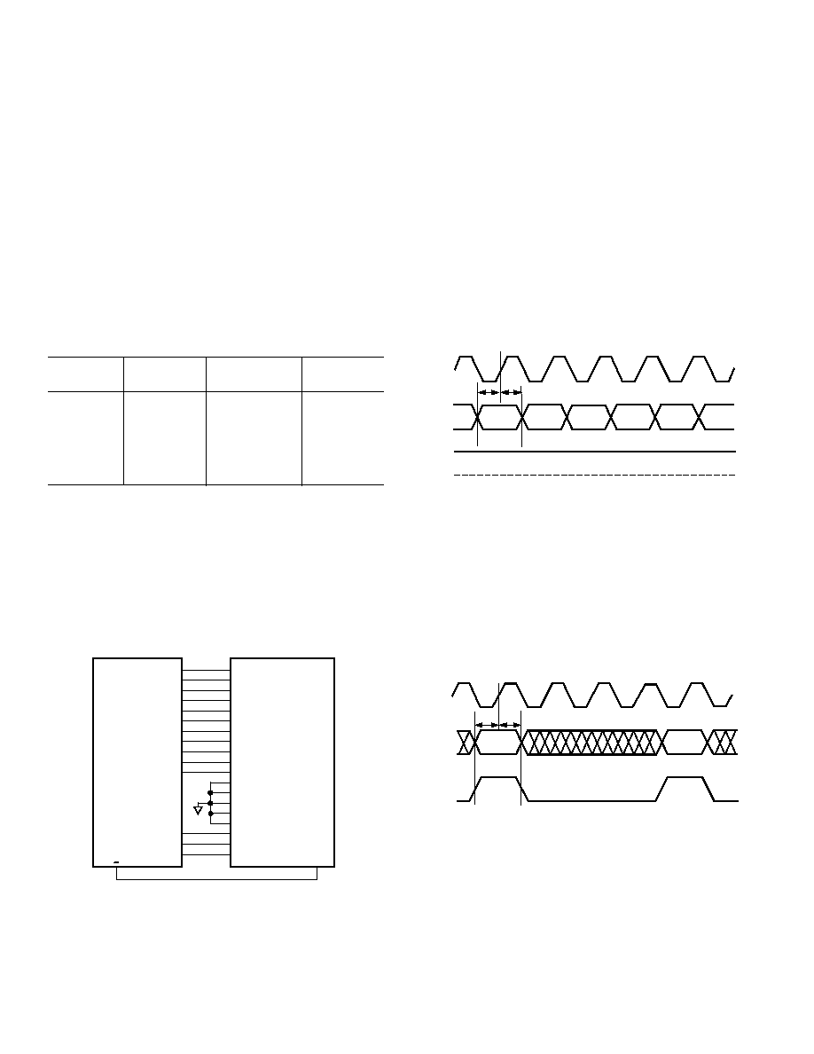
Input Timing
The CLK signal is used to sample the input port and clock the
synchronous signal processing stages that follow. The CLK signal
can operate up to 67 MHz and have a duty cycle of 45% to
55%. In applications using high speed ADCs, the ADC sample
clock is typically used to clock the AD6620. Applications that
require a faster signal processing clock than the ADC sample
clock, may employ fractional rate input timing as shown in the
following sections. The input timing requirements vary according
to the mode of operation. Fractional rate input timing creates a
longer “don’t care” time for the input data so that slower ADCs
need only meet the setup-and-hold conditions for their data
with respect to their own sample clock cycle, rather than the
faster signal processing clock. The ADC sample clock may be
any integer fraction of CLK up to and including 1, as long as
the clock and data rate are less than or equal to 67 MSPS.
Single Channel Real Mode
In the Single Channel Real mode the A/B input pin functions as
an active high input enable. If the A/D sample clock is fast enough
to perform the necessary filter functions, full rate input timing
can be used and A/B should be tied high as shown in Figure 23.
N
N+1
N+2
N+3
N+4
tSI
tHI
CLK
IN[15:0]
EXP[2:0]
A/B
Figure 23. Full Rate Input Timing, Single Channel
Real Mode
When a faster processing clock is used to achieve better filter
performance, the A/D data must be synchronized with the faster
AD6620 CLK signal. This is achieved by having the ADC clock
rate an integer fraction of the AD6620 clock rate. AD6620 input
data is sampled at the slower ADC clock rate. In the Single
Channel Real Mode this is achieved by dynamically controlling
the A/B input and bringing it high before each rising CLK edge
that data is to be sampled on. A/B must be returned low before
the next high speed clock pulse and the duty cycle of the A/B
signal will therefore be equal to the data-to-clock ratio.
N
N+1
tSI
tHI
CLK
IN[15:0]
EXP[2:0]
A/B
Figure 24. Fractional Rate Input Timing (4
× CLK), Single
Channel Real Mode
Diversity Channel Real Mode
In the Diversity Channel Real mode the A/B pin serves not only
as an input enable but also to determine which channel is being
sampled on a given CLK edge. A high on the A/B pin marks
channel A data and a low on A/B marks channel B data. The
AD6620 only accepts the first sample after an A/B transition.
All subsequent samples are disregarded until A/B changes again.
When full rate input timing is employed in the Diversity Chan-
nel Real mode, A/B must toggle on every rising edge of CLK for
new data to be clocked into the AD6620.
相关PDF资料 |
PDF描述 |
|---|---|
| 6274291-2 | CONN JACK VERT PCB 75 OHM BNC |
| AD7669JNZ | IC I/O PORT 8BIT ANLG 28DIP |
| D38999/24FF11PA | CONN RCPT 11POS JAM NUT W/PINS |
| D38999/20JE26HN | CONN RCPT 26POS WALL MNT W/PINS |
| AD7569KNZ | IC I/O PORT 8BIT ANALOG 24DIP |
相关代理商/技术参数 |
参数描述 |
|---|---|
| AD6620PCB | 制造商:AD 制造商全称:Analog Devices 功能描述:65 MSPS Digital Receive Signal Processor |
| AD6620S | 制造商:AD 制造商全称:Analog Devices 功能描述:65 MSPS Digital Receive Signal Processor |
| AD6620S/PCB | 制造商:Analog Devices 功能描述:DUAL CHANNEL DECIMATING RECEIV 制造商:Analog Devices 功能描述:SGNL PROCESSOR 169CSPBGA - Bulk |
| AD6622 | 制造商:AD 制造商全称:Analog Devices 功能描述:Four-Channel, 75 MSPS Digital Transmit Signal Processor TSP |
| AD6622AS | 制造商:Analog Devices 功能描述:Transmit Signal Processor 128-Pin MQFP 制造商:Rochester Electronics LLC 功能描述:4 CHANNEL 65 MSPS DIGITAL UPCONVERTER - Bulk |
发布紧急采购,3分钟左右您将得到回复。