- 您现在的位置:买卖IC网 > PDF目录11767 > AD6620ASZ-REEL (Analog Devices Inc)IC DGTL RCVR DUAL 67MSPS 80-PQFP PDF资料下载
参数资料
| 型号: | AD6620ASZ-REEL |
| 厂商: | Analog Devices Inc |
| 文件页数: | 18/44页 |
| 文件大小: | 0K |
| 描述: | IC DGTL RCVR DUAL 67MSPS 80-PQFP |
| 标准包装: | 500 |
| 接口: | 并行/串行 |
| 电源电压: | 3 V ~ 3.6 V |
| 封装/外壳: | 80-BQFP |
| 供应商设备封装: | 80-PQFP(14x14) |
| 包装: | 带卷 (TR) |
| 安装类型: | 表面贴装 |
第1页第2页第3页第4页第5页第6页第7页第8页第9页第10页第11页第12页第13页第14页第15页第16页第17页当前第18页第19页第20页第21页第22页第23页第24页第25页第26页第27页第28页第29页第30页第31页第32页第33页第34页第35页第36页第37页第38页第39页第40页第41页第42页第43页第44页
AD6620
–25–
REV. A
The maximum number of taps this filter can calculate, NTAPS, is
given by the equation below. The value NTAPS minus 1 is writ-
ten to the AD6620 internal address space at address 30C hex.
The decimation ratio of this filter, MRCF, may be programmed
from 1 to 32. The input rate into the RCF is fSAMP5. NCH is equal
to two for Diversity Channel Real Input mode; otherwise NCH = 1.
N
fM
f
N
TAPS
CLK
RCF
SAMP
CH
≤
×
min
,
5
256
The RCF coefficients are located in addresses 0x000 to 0x0FF
and are interpreted as 20-bit twos complement numbers. When
writing the coefficient RAM, the lower addresses will be multi-
plied by relatively older data from the CIC5 and the higher
coefficient addresses will be multiplied by relatively newer data
from the CIC5. The coefficients need not be symmetric and the
coefficient length, NTAPS, may be even or odd. If the coefficients
are symmetric, then both sides of the impulse response must be
written into the coefficient RAM.
The RCF stores the data from the CIC5 into a 256
× 36 RAM.
256
× 18 is assigned to I data and 256 × 18 is assigned to Q data.
The RCF uses the RAM as a circular buffer, so that it is difficult
to know in which address a particular data element is stored. To
avoid start-up transients due to undefined data RAM values, the
data RAM should be cleared upon initialization. The RCF
utilizes the number of data RAM locations equal to NTAPS
× N
CH,
rounded up to the nearest even number, starting from address
0x100, so these are the only values that need be cleared.
When the RCF is triggered to calculate a filter output, it starts
by multiplying the oldest value in the data RAM by the first
coefficient (located by the RCFOFF register in address 0x30B).
This value is accumulated with the products of newer data words
multiplied by the subsequent locations in the coefficient RAM
until the coefficient address RCFOFF + NTAPS–1 is reached.
Table V. Three-Tap Filter
Coefficient Address
Impulse Response
Data
0
h(0)
n(0) Newest
1
h(1)
n(1)
2 (NTAPS – 1)
h(2)
n(2) Oldest
The output rate of this filter is determined by the output rate of
the CIC5 stage and MRCF.
f
M
SAMPR
SAMP
RCF
=
5
RCF Coefficient Address Offset
This register at address 30b hex allows the AD6620 to hold
multiple filters in the RAM. However, the sum of the taps
required may not exceed 256 divided by the number of chan-
nels. The RCF will compute the filter from RCF_OFFSET to
(RCF_OFFSET + NTAPS). A single access can then be used to
select which of the filters is used without requiring coefficients
be rewritten.
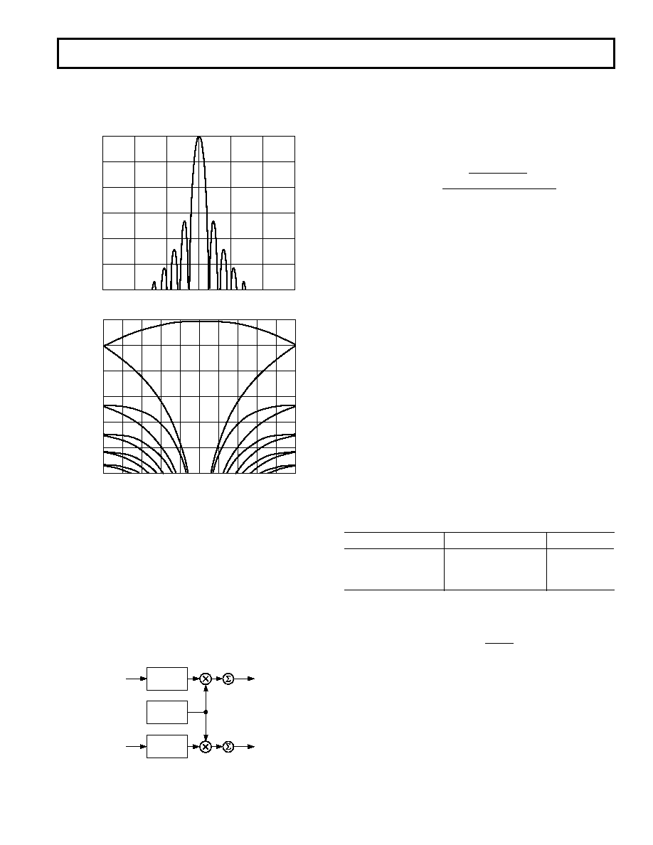
The set of plots below (Figure 39) represents a decimation of 32
in the CIC5 filter. It can be seen that the lobes of the filter drop
as the decimation rate increases, but the aliased frequencies
increase due to the reduction of the output rate.
–120
–100
–80
–60
–40
–20
0
dBFS
f/fSAMP
–0.3
–0.2
–0.1
0.1
0.2
0.3
0
–0.5
–120
–100
–80
–60
–40
–20
0
dBFS
f/fSAMP5
–0.4 –0.3
–0.2
–0.1
0.1
0.2
0.3
0.4
0.5
0
Figure 39. CIC5 Alias Rejection, MCIC5 = 32
RAM COEFFICIENT FILTER
The final signal processing stage is a sum-of-products decimat-
ing filter with programmable coefficients. Figure 40 shows a
simplified block diagram. The data memories I-RAM and Q-RAM
store the 256 most recent complex samples from the previous filter
stage with 18-bit resolution. The coefficient memory, C-RAM,
stores up to 256 coefficients with 20-bit resolution. On each
CLK cycle one tap for I and one tap for Q is calculated using
the same coefficients. The I and Q accumulators provide 3 bits
of headroom. This headroom allows the output of the RCF filter
to contain 23 significant bits.
IIN
QIN
IOUT
QOUT
256 18b
I-RAM
256 20b
C-RAM
256 18b
Q-RAM
Figure 40. RAM Coefficient Filter Block Diagram
相关PDF资料 |
PDF描述 |
|---|---|
| 6274291-2 | CONN JACK VERT PCB 75 OHM BNC |
| AD7669JNZ | IC I/O PORT 8BIT ANLG 28DIP |
| D38999/24FF11PA | CONN RCPT 11POS JAM NUT W/PINS |
| D38999/20JE26HN | CONN RCPT 26POS WALL MNT W/PINS |
| AD7569KNZ | IC I/O PORT 8BIT ANALOG 24DIP |
相关代理商/技术参数 |
参数描述 |
|---|---|
| AD6620PCB | 制造商:AD 制造商全称:Analog Devices 功能描述:65 MSPS Digital Receive Signal Processor |
| AD6620S | 制造商:AD 制造商全称:Analog Devices 功能描述:65 MSPS Digital Receive Signal Processor |
| AD6620S/PCB | 制造商:Analog Devices 功能描述:DUAL CHANNEL DECIMATING RECEIV 制造商:Analog Devices 功能描述:SGNL PROCESSOR 169CSPBGA - Bulk |
| AD6622 | 制造商:AD 制造商全称:Analog Devices 功能描述:Four-Channel, 75 MSPS Digital Transmit Signal Processor TSP |
| AD6622AS | 制造商:Analog Devices 功能描述:Transmit Signal Processor 128-Pin MQFP 制造商:Rochester Electronics LLC 功能描述:4 CHANNEL 65 MSPS DIGITAL UPCONVERTER - Bulk |
发布紧急采购,3分钟左右您将得到回复。