- 您现在的位置:买卖IC网 > PDF目录11767 > AD6620ASZ-REEL (Analog Devices Inc)IC DGTL RCVR DUAL 67MSPS 80-PQFP PDF资料下载
参数资料
| 型号: | AD6620ASZ-REEL |
| 厂商: | Analog Devices Inc |
| 文件页数: | 13/44页 |
| 文件大小: | 0K |
| 描述: | IC DGTL RCVR DUAL 67MSPS 80-PQFP |
| 标准包装: | 500 |
| 接口: | 并行/串行 |
| 电源电压: | 3 V ~ 3.6 V |
| 封装/外壳: | 80-BQFP |
| 供应商设备封装: | 80-PQFP(14x14) |
| 包装: | 带卷 (TR) |
| 安装类型: | 表面贴装 |
第1页第2页第3页第4页第5页第6页第7页第8页第9页第10页第11页第12页当前第13页第14页第15页第16页第17页第18页第19页第20页第21页第22页第23页第24页第25页第26页第27页第28页第29页第30页第31页第32页第33页第34页第35页第36页第37页第38页第39页第40页第41页第42页第43页第44页
AD6620
–20–
REV. A
modes, fSAMP is equal to fCLK multiplied by the fraction of CLK
cycles on which A/B has been toggled. The NCO worst case
discrete spur is better than –100 dBc for all output frequencies.
The control word, NCO_FREQ is interpreted as a 32-bit unsigned
integer. To translate a channel centered at fCH to dc, calculate
NCO_FREQ using the equation below. The mod function is
used here to allow for Super Nyquist sampling where the IF
carrier (fCH) is larger than the sample rate (fSAMP). The mod
removes the integer portion of the number and forces it into the
32-bit NCO Frequency Register. If the fraction remaining is
larger than 0.5, the NCO will be tuning above the Nyquist rate.
The corresponding signal is then aliased back into the first Nyquist
Zone as a negative frequency.
NCO
FREQ
f
CH
SAMP
_,
=×
21
32
mod
In both Single and Diversity Channel Real Input modes, the out-
put of the translation stage is the complex product of the real
input samples and the complex samples from the NCO. It is
necessary for the subsequent decimating filters to reject the
unwanted image of the channel of interest, as well as any unwanted
neighboring signals (and their images) not rejected by previ-
ous analog filters.
In the Diversity Channel Real Input mode, the same NCO output
words are used for both channel A and B streams, resulting in
identical phase shifts. In Single Channel Complex mode both I
and Q inputs are multiplied by the quadrature outputs of the
NCO. The I and Q products of the multiply are then processed
in the AD6620 filter stages.
In single channel real or dual channel real operation, the frequency
translation and filtering processes provide a gain of –6 dB. This
can be visualized since the input data is usually a real sampled
signal consisting of both positive and negative frequency compo-
nents (Figure 2a). After being mixed with the complex NCO,
the normal filtering of the AD6620 will remove one component
or the other resulting in an analytic signal (Figure 2b). This
filtering thus removes one-half or 6 dB of the signal keeping
consistent with the mathematics involved. If however, the filter-
ing of the device allows both the positive and negative frequency
components to pass (i.e., the original signal is near dc), the gain
of the frequency translation is 0 dB. Finally, if the NCO is
bypassed, the gain of the frequency translation block is –12 dB.
Phase Dither
The AD6620 provides a phase dither option for improving the
spurious performance of the NCO. This is controlled via the
NCO Control Register at address 301 hex. When phase dither is
enabled by setting Bit 1 of this register high, spurs due to phase
truncation in the NCO are randomized. The energy from these
spurs is spread into the noise floor and Spurious Free Dynamic
Range is increased at the expense of very slight decreases in the
SNR. Phase dither should be experimented with for each desired
NCO frequency and if it is seen to reduce spurs, it should be
considered. The choice of whether Phase Dither is used in a
system will ultimately be decided by the system goals. If lower
spurs are desired at the expense of a slightly raised noise floor, it
should be employed. If a low noise floor is desired and the higher
spurs can be tolerated or filtered by subsequent stages, then
Phase Dither is not needed.
Amplitude Dither
The second dither option is Amplitude Dither or “Complex
Dither.” Amplitude Dither is enabled by setting Bit 2 of the
NCO Control Register at address 0x301 high. Amplitude Dither
improves performance by randomizing the amplitude quantiza-
tion errors within the angular to Cartesian conversion of the
NCO. This dither will be particularly useful when the NCO
frequency is close to an integer submultiple of the Input Data
Rate. However, this option may reduce spurs at the expense of a
slightly raised noise floor. Amplitude Dither and Phase Dither
can be used together, separately or not at all.
Phase Offset
The phase offset register adds an offset to the phase accumula-
tor of the NCO. This is a 16-bit register and is interpreted as a
16-bit unsigned integer. A 0 in this register corresponds to a 0
Radian offset and an FFFF hex corresponds to an offset of 2
π
(1 – 1/(2^16)) Radians. This register can be used to allow mul-
tiple AD6620s whose NCOs are synchronized to produce sine
waves with a known and steady phase difference.
NCO Synchronization
In order to achieve phase coherence between several AD6620s,
a SYNC_NCO pin is provided. When the internal register
bit, SYNC_M/S (Bit 3 of internal register 0x300), is set high,
SYNC_NCO provides a synchronization pulse on the rising
edge of CLK. When the SYNC_M/S bit is low, SYNC_NCO
accepts an external synchronization signal sampled on the rising
edge of CLK. When the AD6620 is a slave, the SYNC_NCO
signal need not be a short pulse. It may be taken high and held
for more than a CLK cycle in which case the NCO will be held
inactive until this pin is again lowered. If the device is run as a
sync slave in Single Channel Mode, the SYNC_NCO pin must
be held low for one sample period, usually one clock cycle. If the
device is run in Diversity Channel Real mode, the SYNC_NCO
must be high for two sample periods (clock cycles). In a system
with an array of AD6620s it is not necessary to use one as a
master. It may be desirable to generate a synchronization signal
elsewhere in the system and use that to control the AD6620. An
example of this may be in systems that receive packets of data.
In this case, the NCO may be resynchronized prior to the begin-
ning of the packet, thus giving a consistent phase relationship on
each burst. This allows for ease of use in a large system where
many AD6620s need be synchronized accurately across a large
backplane or installation.
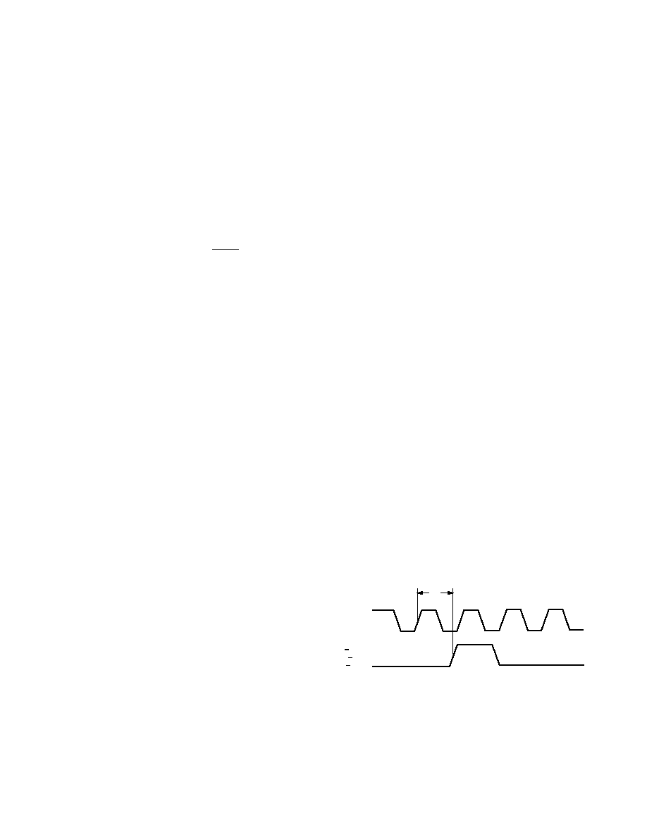
tDY
CLK
SYNC NCO
SYNC CIC
SYNC RCF
NOTE:
IN THE SLAVE MODE WITH SINGLE CHANNEL OPERATION, THE WIDTH
OF THE SYNC_NCO SHOULD BE ONE SAMPLE CLOCK CYCLE. IN DUAL
CHANNEL MODE, THE PULSEWIDTH SHOULD BE TWO SAMPLE CLOCK
CYCLES. IF A PULSE LONGER THAN SPECIFIED IS USED, THE NCO WILL
BE INHIBITED AND NOT INCREMENT PROPERLY.
Figure 34. SYNC_NCO Pin
相关PDF资料 |
PDF描述 |
|---|---|
| 6274291-2 | CONN JACK VERT PCB 75 OHM BNC |
| AD7669JNZ | IC I/O PORT 8BIT ANLG 28DIP |
| D38999/24FF11PA | CONN RCPT 11POS JAM NUT W/PINS |
| D38999/20JE26HN | CONN RCPT 26POS WALL MNT W/PINS |
| AD7569KNZ | IC I/O PORT 8BIT ANALOG 24DIP |
相关代理商/技术参数 |
参数描述 |
|---|---|
| AD6620PCB | 制造商:AD 制造商全称:Analog Devices 功能描述:65 MSPS Digital Receive Signal Processor |
| AD6620S | 制造商:AD 制造商全称:Analog Devices 功能描述:65 MSPS Digital Receive Signal Processor |
| AD6620S/PCB | 制造商:Analog Devices 功能描述:DUAL CHANNEL DECIMATING RECEIV 制造商:Analog Devices 功能描述:SGNL PROCESSOR 169CSPBGA - Bulk |
| AD6622 | 制造商:AD 制造商全称:Analog Devices 功能描述:Four-Channel, 75 MSPS Digital Transmit Signal Processor TSP |
| AD6622AS | 制造商:Analog Devices 功能描述:Transmit Signal Processor 128-Pin MQFP 制造商:Rochester Electronics LLC 功能描述:4 CHANNEL 65 MSPS DIGITAL UPCONVERTER - Bulk |
发布紧急采购,3分钟左右您将得到回复。