- 您现在的位置:买卖IC网 > PDF目录1986 > AD9510BCPZ-REEL7 (Analog Devices Inc)IC CLOCK DIST 8OUT PLL 64LFCSP PDF资料下载
参数资料
| 型号: | AD9510BCPZ-REEL7 |
| 厂商: | Analog Devices Inc |
| 文件页数: | 21/56页 |
| 文件大小: | 0K |
| 描述: | IC CLOCK DIST 8OUT PLL 64LFCSP |
| 标准包装: | 750 |
| 类型: | 扇出缓冲器(分配),除法器 |
| PLL: | 是 |
| 输入: | 时钟 |
| 输出: | CMOS,LVDS,LVPECL |
| 电路数: | 1 |
| 比率 - 输入:输出: | 2:8 |
| 差分 - 输入:输出: | 是/是 |
| 频率 - 最大: | 1.2GHz |
| 除法器/乘法器: | 是/无 |
| 电源电压: | 3.135 V ~ 3.465 V |
| 工作温度: | -40°C ~ 85°C |
| 安装类型: | 表面贴装 |
| 封装/外壳: | 64-VFQFN 裸露焊盘,CSP |
| 供应商设备封装: | 64-LFCSP-VQ(9x9) |
| 包装: | 带卷 (TR) |
| 配用: | AD9510-VCO/PCBZ-ND - BOARD EVALUATION FOR AD9510 AD9510/PCBZ-ND - BOARD EVALUATION FOR AD9510 |
第1页第2页第3页第4页第5页第6页第7页第8页第9页第10页第11页第12页第13页第14页第15页第16页第17页第18页第19页第20页当前第21页第22页第23页第24页第25页第26页第27页第28页第29页第30页第31页第32页第33页第34页第35页第36页第37页第38页第39页第40页第41页第42页第43页第44页第45页第46页第47页第48页第49页第50页第51页第52页第53页第54页第55页第56页
AD9510
Data Sheet
Rev. B | Page 28 of 56
FUNCTIONAL DESCRIPTION
OVERALL
Figure 33 shows a block diagram of the AD9510. The chip
combines a programmable PLL core with a configurable clock
distribution system. A complete PLL requires the addition of a
suitable external VCO (or VCXO) and loop filter. This PLL can
lock to a reference input signal and produce an output that is
related to the input frequency by the ratio defined by the pro-
grammable R and N dividers. The PLL cleans up some jitter
from the external reference signal, depending on the loop band-
width and the phase noise performance of the VCO (VCXO).
The output from the VCO (VCXO) can be applied to the clock
distribution section of the chip, where it can be divided by any
integer value from 1 to 32. The duty cycle and relative phase of
the outputs can be selected. There are four LVPECL outputs,
(OUT0, OUT1, OUT2, and OUT3) and four outputs that can be
either LVDS or CMOS level outputs (OUT4, OUT5, OUT6, and
OUT7). Two of these outputs (OUT5 and OUT6) can also make
use of a variable delay block.
Alternatively, the clock distribution section can be driven directly
by an external clock signal, and the PLL can be powered off.
Whenever the clock distribution section is used alone, there is
no clock cleanup. The jitter of the input clock signal is passed
along directly to the distribution section and may dominate at
the clock outputs.
PLL SECTION
The AD9510 consists of a PLL section and a distribution section.
If desired, the PLL section can be used separately from the
distribution section.
The AD9510 has a complete PLL core on-chip, requiring only
an external loop filter and VCO/VCXO. This PLL is based on
the ADF4106, a PLL noted for its superb low phase noise per-
formance. The operation of the AD9510 PLL is nearly identical
to that of the ADF4106, offering an advantage to those with
experience with the ADF series of PLLs. Differences include the
addition of differential inputs at REFIN and CLK2, a different
control register architecture. Also, the prescaler is changed to
allow N as low as 1. The AD9510 PLL implements the digital
lock detect feature somewhat differently than the ADF4106
does, offering improved functionality at higher PFD rates. See
the Register Map Description section.
PLL Reference Input—REFIN
The REFIN/REFINB pins can be driven by either a differential
or a single-ended signal. These pins are internally self-biased so
that they can be ac-coupled via capacitors. It is possible to dc-
couple to these inputs. If REFIN is driven single-ended, decouple
the unused side (REFINB) via a suitable capacitor to a quiet
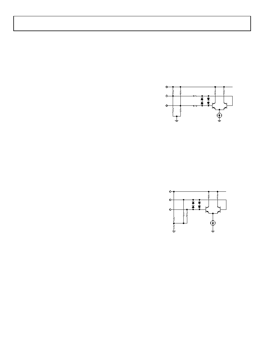
ground. Figure 34 shows the equivalent circuit of REFIN.
Figure 34. REFIN Equivalent Circuit
VCO/VCXO Clock Input—CLK2
The CLK2 differential input is used to connect an external
VCO or VCXO to the PLL. Only the CLK2 input port has a
connection to the PLL N divider. This input can receive up to
1.6 GHz. These inputs are internally self-biased and must be
ac-coupled via capacitors.
Alternatively, CLK2 can be used as an input to the distribution
section. This is accomplished by setting Register 0x45[0] = 0b.
The default condition is for CLK1 to feed the distribution section.
Figure 35. CLK1, CLK2 Equivalent Input Circuit
PLL Reference Divider—R
The REFIN/REFINB inputs are routed to reference divider, R,
which is a 14-bit counter. R can be programmed to any value
from 1 to 16383 (a value of 0 results in a divide by 1) via its
control register (Register 0x0B[5:0], Register 0x0C[7:0]). The
output of the R divider goes to one of the phase frequency
detector inputs. Do not exceed the maximum allowable frequency
into the phase frequency detector (PFD). This means that the
REFIN frequency divided by R must be less than the maximum
allowable PFD frequency. See Figure 34.
05046-033
VS
REFIN
REFINB
150
150
10k
12k
10k
10k
05046-016
VS
CLOCK INPUT
STAGE
CLK
CLKB
5k
5k
2.5k
2.5k
相关PDF资料 |
PDF描述 |
|---|---|
| AD9511BCPZ-REEL7 | IC CLOCK DIST 5OUT PLL 48LFCSP |
| AD9512UCPZ-EP-R7 | IC CLOCK DIST 5OUT PLL 48LFCSP |
| AD9512UCPZ-EP | IC CLOCK DIST 5OUT PLL 48LFCSP |
| AD9513BCPZ-REEL7 | IC CLOCK DIST 3OUT PLL 32LFCSP |
| AD9514BCPZ-REEL7 | IC CLOCK DIST 3OUT PLL 32LFCSP |
相关代理商/技术参数 |
参数描述 |
|---|---|
| AD9510-VCO/PCB | 制造商:Analog Devices 功能描述:EVAL BD FOR 1.2 GHZ CLOCK DISTRIBUTION IC, PLL CORE, DIVIDER - Bulk 制造商:Analog Devices 功能描述:IC ((NS)) |
| AD9510-VCO/PCBZ | 功能描述:BOARD EVALUATION FOR AD9510 RoHS:是 类别:编程器,开发系统 >> 评估演示板和套件 系列:- 标准包装:1 系列:PSoC® 主要目的:电源管理,热管理 嵌入式:- 已用 IC / 零件:- 主要属性:- 次要属性:- 已供物品:板,CD,电源 |
| AD9511 | 制造商:AD 制造商全称:Analog Devices 功能描述:1.2 GHz Clock Distribution IC, PLL Core, Dividers, Delay Adjust, Five Outputs |
| AD9511/PCB | 制造商:Analog Devices 功能描述:1.2 GHZ CLOCK DISTRIBUTION IC, PLL CORE,DIVIDERS, DELAY ADJUST, FIVE OUTPUTS 制造商:Analog Devices 功能描述:EVAL BD FOR AD9511 1.2 GHZ CLOCK DISTRIBUTION IC, PLL CORE,D - Bulk |
| AD9511BCPZ | 功能描述:IC CLOCK DIST 5OUT PLL 48LFCSP RoHS:是 类别:集成电路 (IC) >> 时钟/计时 - 时钟发生器,PLL,频率合成器 系列:- 标准包装:1,000 系列:Precision Edge® 类型:时钟/频率合成器 PLL:无 输入:CML,PECL 输出:CML 电路数:1 比率 - 输入:输出:2:1 差分 - 输入:输出:是/是 频率 - 最大:10.7GHz 除法器/乘法器:无/无 电源电压:2.375 V ~ 3.6 V 工作温度:-40°C ~ 85°C 安装类型:表面贴装 封装/外壳:16-VFQFN 裸露焊盘,16-MLF? 供应商设备封装:16-MLF?(3x3) 包装:带卷 (TR) 其它名称:SY58052UMGTRSY58052UMGTR-ND |
发布紧急采购,3分钟左右您将得到回复。