- 您现在的位置:买卖IC网 > PDF目录1986 > AD9511BCPZ-REEL7 (Analog Devices Inc)IC CLOCK DIST 5OUT PLL 48LFCSP PDF资料下载
参数资料
| 型号: | AD9511BCPZ-REEL7 |
| 厂商: | Analog Devices Inc |
| 文件页数: | 1/60页 |
| 文件大小: | 0K |
| 描述: | IC CLOCK DIST 5OUT PLL 48LFCSP |
| 标准包装: | 750 |
| 类型: | 扇出缓冲器(分配),除法器 |
| PLL: | 是 |
| 输入: | 时钟 |
| 输出: | CMOS,LVDS,LVPECL |
| 电路数: | 1 |
| 比率 - 输入:输出: | 2:5 |
| 差分 - 输入:输出: | 是/是 |
| 频率 - 最大: | 1.2GHz |
| 除法器/乘法器: | 是/无 |
| 电源电压: | 3.135 V ~ 3.465 V |
| 工作温度: | -40°C ~ 85°C |
| 安装类型: | 表面贴装 |
| 封装/外壳: | 48-VFQFN 裸露焊盘,CSP |
| 供应商设备封装: | 48-LFCSP-VQ(7x7) |
| 包装: | 带卷 (TR) |
当前第1页第2页第3页第4页第5页第6页第7页第8页第9页第10页第11页第12页第13页第14页第15页第16页第17页第18页第19页第20页第21页第22页第23页第24页第25页第26页第27页第28页第29页第30页第31页第32页第33页第34页第35页第36页第37页第38页第39页第40页第41页第42页第43页第44页第45页第46页第47页第48页第49页第50页第51页第52页第53页第54页第55页第56页第57页第58页第59页第60页
1.2 GHz Clock Distribution IC, PLL Core,
Dividers, Delay Adjust, Five Outputs
AD9511
Rev. A
Information furnished by Analog Devices is believed to be accurate and reliable.
However, no responsibility is assumed by Analog Devices for its use, nor for any
infringements of patents or other rights of third parties that may result from its use.
Specifications subject to change without notice. No license is granted by implication
or otherwise under any patent or patent rights of Analog Devices. Trademarks and
registered trademarks are the property of their respective owners.
One Technology Way, P.O. Box 9106, Norwood, MA 02062-9106, U.S.A.
Tel: 781.329.4700
www.analog.com
Fax: 781.461.3113
2005 Analog Devices, Inc. All rights reserved.
FEATURES
Low phase noise phase-locked loop core
Reference input frequencies to 250 MHz
Programmable dual-modulus prescaler
Programmable charge pump (CP) current
Separate CP supply (VCPS) extends tuning range
Two 1.6 GHz, differential clock inputs
5 programmable dividers, 1 to 32, all integers
Phase select for output-to-output coarse delay adjust
3 independent 1.2 GHz LVPECL outputs
Additive output jitter 225 fs rms
2 independent 800 MHz/250 MHz LVDS/CMOS clock outputs
Additive output jitter 275 fs rms
Fine delay adjust on 1 LVDS/CMOS output
Serial control port
Space-saving 48-lead LFCSP
APPLICATIONS
Low jitter, low phase noise clock distribution
Clocking high speed ADCs, DACs, DDSs, DDCs, DUCs, MxFEs
High performance wireless transceivers
High performance instrumentation
Broadband infrastructure
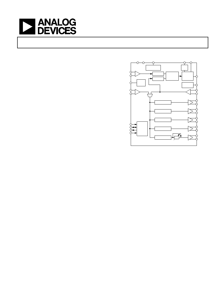
FUNCTIONAL BLOCK DIAGRAM
05286-001
R DIVIDER
N DIVIDER
PHASE
FREQUENCY
DETECTOR
CHARGE
PUMP
PLL
SETTINGS
CLK2
STATUS
CLK2B
PROGRAMMABLE
DIVIDERS AND
PHASE ADJUST
OUT0
OUT0B
LVPECL
/1, /2, /3... /31, /32
OUT1
OUT1B
LVPECL
/1, /2, /3... /31, /32
OUT2
OUT2B
LVPECL
/1, /2, /3... /31, /32
OUT3
OUT3B
LVDS/CMOS
/1, /2, /3... /31, /32
OUT4
OUT4B
LVDS/CMOS
/1, /2, /3... /31, /32
DELAY
ADJUST
ΔT
CLK1
CLK1B
REFIN
REFINB
FUNCTION
SCLK
SDIO
SDO
CSB
SERIAL
CONTROL
PORT
CP
CPRSET
DISTRIBUTION
REF
SYNCB,
RESETB
PDB
RSET
AD9511
GND
VS
VCP
PLL
REF
Figure 1.
GENERAL DESCRIPTION
The AD9511 provides a multi-output clock distribution
function along with an on-chip PLL core. The design
emphasizes low jitter and phase noise to maximize data
converter performance. Other applications with demanding
phase noise and jitter requirements also benefit from this part.
The PLL section consists of a programmable reference divider
(R); a low noise phase frequency detector (PFD); a precision
charge pump (CP); and a programmable feedback divider (N).
By connecting an external VCXO or VCO to the CLK2/CLK2B
pins, frequencies up to 1.6 GHz may be synchronized to the
input reference.
There are five independent clock outputs. Three outputs are
LVPECL (1.2 GHz), and two are selectable as either LVDS
(800 MHz) or CMOS (250 MHz) levels.
Each output has a programmable divider that may be bypassed
or set to divide by any integer up to 32. The phase of one clock
output relative to another clock output may be varied by means
of a divider phase select function that serves as a coarse timing
adjustment. One of the LVDS/CMOS outputs features a
programmable delay element with full-scale ranges up to 10 ns
of delay. This fine tuning delay block has 5-bit resolution, giving
32 possible delays from which to choose for each full-scale
setting.
The AD9511 is ideally suited for data converter clocking
applications where maximum converter performance is
achieved by encode signals with subpicosecond jitter.
The AD9511 is available in a 48-lead LFCSP and can be
operated from a single 3.3 V supply. An external VCO, which
requires an extended voltage range, can be accommodated by
connecting the charge pump supply (VCP) to 5.5 V. The
temperature range is 40°C to +85°C.
相关PDF资料 |
PDF描述 |
|---|---|
| AD9512UCPZ-EP-R7 | IC CLOCK DIST 5OUT PLL 48LFCSP |
| AD9512UCPZ-EP | IC CLOCK DIST 5OUT PLL 48LFCSP |
| AD9513BCPZ-REEL7 | IC CLOCK DIST 3OUT PLL 32LFCSP |
| AD9514BCPZ-REEL7 | IC CLOCK DIST 3OUT PLL 32LFCSP |
| AD9515BCPZ-REEL7 | IC CLOCK DIST 2OUT PLL 32LFCSP |
相关代理商/技术参数 |
参数描述 |
|---|---|
| AD9511-VCO/PCB | 制造商:Analog Devices 功能描述:EVAL BD FOR AD9511 1.2 GHZ CLOCK DISTRIBUTION IC, PLL CORE,D - Bulk |
| AD9512 | 制造商:AD 制造商全称:Analog Devices 功能描述:800 MHz Clock Distribution IC,1.5 GHz Inputs, Dividers, Delay Adjust, Five Outputs |
| AD9512/PCB | 制造商:Analog Devices 功能描述:Evaluation Kit For 1.2 GHZ Clock Distribution IC, 1.6 GHZ Inputs, Dividers, Delay Adjust, Five Outputs 制造商:Analog Devices 功能描述:EVAL KIT FOR 1.2 GHZ CLOCK DISTRIBUTION IC, 1.6 GHZ INPUTS, - Bulk |
| AD9512/PCBZ | 功能描述:BOARD EVAL FOR AD9512 RoHS:是 类别:编程器,开发系统 >> 评估演示板和套件 系列:- 标准包装:1 系列:PSoC® 主要目的:电源管理,热管理 嵌入式:- 已用 IC / 零件:- 主要属性:- 次要属性:- 已供物品:板,CD,电源 |
| AD9512BCPZ | 功能描述:IC CLOCK DIST 5OUT PLL 48LFCSP RoHS:是 类别:集成电路 (IC) >> 时钟/计时 - 时钟发生器,PLL,频率合成器 系列:- 标准包装:2,000 系列:- 类型:PLL 时钟发生器 PLL:带旁路 输入:LVCMOS,LVPECL 输出:LVCMOS 电路数:1 比率 - 输入:输出:2:11 差分 - 输入:输出:是/无 频率 - 最大:240MHz 除法器/乘法器:是/无 电源电压:3.135 V ~ 3.465 V 工作温度:0°C ~ 70°C 安装类型:表面贴装 封装/外壳:32-LQFP 供应商设备封装:32-TQFP(7x7) 包装:带卷 (TR) |
发布紧急采购,3分钟左右您将得到回复。