- 您现在的位置:买卖IC网 > PDF目录1986 > AD9511BCPZ-REEL7 (Analog Devices Inc)IC CLOCK DIST 5OUT PLL 48LFCSP PDF资料下载
参数资料
| 型号: | AD9511BCPZ-REEL7 |
| 厂商: | Analog Devices Inc |
| 文件页数: | 42/60页 |
| 文件大小: | 0K |
| 描述: | IC CLOCK DIST 5OUT PLL 48LFCSP |
| 标准包装: | 750 |
| 类型: | 扇出缓冲器(分配),除法器 |
| PLL: | 是 |
| 输入: | 时钟 |
| 输出: | CMOS,LVDS,LVPECL |
| 电路数: | 1 |
| 比率 - 输入:输出: | 2:5 |
| 差分 - 输入:输出: | 是/是 |
| 频率 - 最大: | 1.2GHz |
| 除法器/乘法器: | 是/无 |
| 电源电压: | 3.135 V ~ 3.465 V |
| 工作温度: | -40°C ~ 85°C |
| 安装类型: | 表面贴装 |
| 封装/外壳: | 48-VFQFN 裸露焊盘,CSP |
| 供应商设备封装: | 48-LFCSP-VQ(7x7) |
| 包装: | 带卷 (TR) |
第1页第2页第3页第4页第5页第6页第7页第8页第9页第10页第11页第12页第13页第14页第15页第16页第17页第18页第19页第20页第21页第22页第23页第24页第25页第26页第27页第28页第29页第30页第31页第32页第33页第34页第35页第36页第37页第38页第39页第40页第41页当前第42页第43页第44页第45页第46页第47页第48页第49页第50页第51页第52页第53页第54页第55页第56页第57页第58页第59页第60页
AD9511
Rev. A | Page 47 of 60
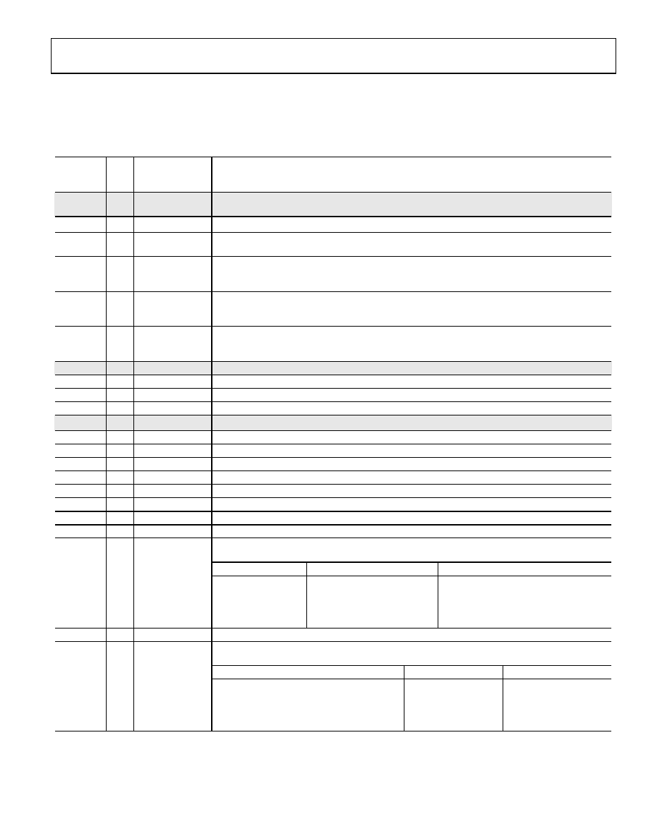
REGISTER MAP DESCRIPTION
Table 24 lists the AD9511 control registers by hexadecimal address. A specific bit or range of bits within a register is indicated by angle
brackets. For example, <3> refers to Bit 3, while <5:2> refers to the range of bits from Bit 5 through Bit 2. Table 24 describes the
functionality of the control registers on a bit-by-bit basis. For a more concise (but less descriptive) table, see Table 23.
Table 24. AD9511 Register Descriptions
Reg.
Addr.
(Hex)
Bit(s) Name
Description
Serial Control Port
Configuration
Any changes to this register takes effect immediately. Register 5Ah<0> Update Registers does not
have to be written.
00
<3:0>
Not Used.
00
<4>
Long Instruction
When this bit is set (1), the instruction phase is 16 bits. When clear (0), the instruction phase is 8 bits.
The default, and only, mode for this part is long instruction (Default = 1b).
00
<5>
Soft Reset
When this bit is set (1), the chip executes a soft reset, restoring default values to the internal
registers, except for this register, 00h. This bit is not self-clearing. A clear (0) has to be written
to it to clear it.
00
<6>
LSB First
When this bit is set (1), the input and output data is oriented as LSB first. Additionally, register
addressing increments. If this bit is clear (0), data is oriented as MSB first and register addressing
decrements. (Default = 0b, MSB first).
00
<7>
SDO Inactive
(Bidirectional
Mode)
When set (1), the SDO pin is tri-state and all read data goes to the SDIO pin. When clear (0), the
SDO is active (unidirectional mode). (Default = 0b).
Not Used
01
<7:0>
Not Used.
02
<7:0>
Not Used.
03
<7:0>
Not Used.
PLL Settings
04
<5:0> A Counter
6-Bit A Counter <5:0>.
04
<7:6>
Not Used.
05
<4:0> B Counter MSBs
13-Bit B Counter (MSB) <12:8>.
05
<7:5>
Not Used.
06
<7:0> B Counter LSBs
13-Bit B Counter (LSB) <7:0>.
07
<1:0>
Not Used.
07
<2>
LOR Enable
1 = Enables the Loss-of-Reference (LOR) Function; (Default = 0b).
07
<4:3>
Not Used.
07
<6:5> LOR Initial Lock
Detect Delay
LOR Initial Lock Detect Delay. Once a lock detect is indicated, this is the number of phase frequency
detector (PFD) cycles that occur prior to turning on the LOR monitor.
<6>
<5>
LOR Initial Lock Detect Delay
0
3 PFD Cycles (Default)
0
1
6 PFD Cycles
1
0
12 PFD Cycles
1
24 PFD Cycles
07
<7>
Not Used
08
<1:0> Charge Pump
Mode
<1>
<0>
Charge Pump Mode
0
Tri-Stated (Default)
0
1
Pump-Up
1
0
Pump-Down
1
Normal Operation
相关PDF资料 |
PDF描述 |
|---|---|
| AD9512UCPZ-EP-R7 | IC CLOCK DIST 5OUT PLL 48LFCSP |
| AD9512UCPZ-EP | IC CLOCK DIST 5OUT PLL 48LFCSP |
| AD9513BCPZ-REEL7 | IC CLOCK DIST 3OUT PLL 32LFCSP |
| AD9514BCPZ-REEL7 | IC CLOCK DIST 3OUT PLL 32LFCSP |
| AD9515BCPZ-REEL7 | IC CLOCK DIST 2OUT PLL 32LFCSP |
相关代理商/技术参数 |
参数描述 |
|---|---|
| AD9511-VCO/PCB | 制造商:Analog Devices 功能描述:EVAL BD FOR AD9511 1.2 GHZ CLOCK DISTRIBUTION IC, PLL CORE,D - Bulk |
| AD9512 | 制造商:AD 制造商全称:Analog Devices 功能描述:800 MHz Clock Distribution IC,1.5 GHz Inputs, Dividers, Delay Adjust, Five Outputs |
| AD9512/PCB | 制造商:Analog Devices 功能描述:Evaluation Kit For 1.2 GHZ Clock Distribution IC, 1.6 GHZ Inputs, Dividers, Delay Adjust, Five Outputs 制造商:Analog Devices 功能描述:EVAL KIT FOR 1.2 GHZ CLOCK DISTRIBUTION IC, 1.6 GHZ INPUTS, - Bulk |
| AD9512/PCBZ | 功能描述:BOARD EVAL FOR AD9512 RoHS:是 类别:编程器,开发系统 >> 评估演示板和套件 系列:- 标准包装:1 系列:PSoC® 主要目的:电源管理,热管理 嵌入式:- 已用 IC / 零件:- 主要属性:- 次要属性:- 已供物品:板,CD,电源 |
| AD9512BCPZ | 功能描述:IC CLOCK DIST 5OUT PLL 48LFCSP RoHS:是 类别:集成电路 (IC) >> 时钟/计时 - 时钟发生器,PLL,频率合成器 系列:- 标准包装:2,000 系列:- 类型:PLL 时钟发生器 PLL:带旁路 输入:LVCMOS,LVPECL 输出:LVCMOS 电路数:1 比率 - 输入:输出:2:11 差分 - 输入:输出:是/无 频率 - 最大:240MHz 除法器/乘法器:是/无 电源电压:3.135 V ~ 3.465 V 工作温度:0°C ~ 70°C 安装类型:表面贴装 封装/外壳:32-LQFP 供应商设备封装:32-TQFP(7x7) 包装:带卷 (TR) |
发布紧急采购,3分钟左右您将得到回复。