- 您现在的位置:买卖IC网 > PDF目录1986 > AD9511BCPZ-REEL7 (Analog Devices Inc)IC CLOCK DIST 5OUT PLL 48LFCSP PDF资料下载
参数资料
| 型号: | AD9511BCPZ-REEL7 |
| 厂商: | Analog Devices Inc |
| 文件页数: | 35/60页 |
| 文件大小: | 0K |
| 描述: | IC CLOCK DIST 5OUT PLL 48LFCSP |
| 标准包装: | 750 |
| 类型: | 扇出缓冲器(分配),除法器 |
| PLL: | 是 |
| 输入: | 时钟 |
| 输出: | CMOS,LVDS,LVPECL |
| 电路数: | 1 |
| 比率 - 输入:输出: | 2:5 |
| 差分 - 输入:输出: | 是/是 |
| 频率 - 最大: | 1.2GHz |
| 除法器/乘法器: | 是/无 |
| 电源电压: | 3.135 V ~ 3.465 V |
| 工作温度: | -40°C ~ 85°C |
| 安装类型: | 表面贴装 |
| 封装/外壳: | 48-VFQFN 裸露焊盘,CSP |
| 供应商设备封装: | 48-LFCSP-VQ(7x7) |
| 包装: | 带卷 (TR) |
第1页第2页第3页第4页第5页第6页第7页第8页第9页第10页第11页第12页第13页第14页第15页第16页第17页第18页第19页第20页第21页第22页第23页第24页第25页第26页第27页第28页第29页第30页第31页第32页第33页第34页当前第35页第36页第37页第38页第39页第40页第41页第42页第43页第44页第45页第46页第47页第48页第49页第50页第51页第52页第53页第54页第55页第56页第57页第58页第59页第60页
AD9511
Rev. A | Page 40 of 60
Synchronization of two or more AD9511s requires a fast clock
and a slow clock. The fast clock can be up to 1 GHz and may be
the clock driving the master AD9511 CLK1 input or one of the
outputs of the master. The fast clock acts as the input to the
distribution section of the slave AD9511 and is connected to its
CLK1 input. The PLL may be used on the master, but the slave
PLL is not used.
RESET MODES
The AD9511 has several ways to force the chip into a reset
condition.
Power-On Reset—Start-Up Conditions when VS is
Applied
A power-on reset (POR) is issued when the VS power supply is
turned on. This initializes the chip to the power-on conditions
that are determined by the default register settings. These are
indicated in the default value column of Table 23.
The slow clock is the clock that is synchronized across the two
chips. This clock must be no faster than one-fourth of the fast
clock, and no greater than 250 MHz. The slow clock is taken
from one of the outputs of the master AD9511 and acts as the
REFIN (or CLK2) input to the slave AD9511. One of the
outputs of the slave must provide this same frequency back to
the CLK2 (or REFIN) input of the slave.
Asynchronous Reset via the FUNCTION Pin
As mentioned in the FUNCTION Pin section, a hard reset,
RESETB: 58h<6:5> = 00b (Default), restores the chip to the
default settings.
Multichip synchronization is enabled by writing to Register
58h<0> = 1b on the slave AD9511. When this bit is set, the
STATUS pin becomes the output for the SYNC signal. A low
signal indicates an in-sync condition, and a high indicates an
out-of-sync condition.
Soft Reset via the Serial Port
The serial control port allows a soft reset by writing to
Register 00h<5> = 1b. When this bit is set, the chip executes a
soft reset. This restores the default values to the internal
registers, except for Register 00h itself.
Register 58h<1> selects the number of fast clock cycles that are
the maximum separation of the slow clock edges that are
considered synchronized. When 58h<1> = 0b (default), the
slow clock edges must be coincident within 1 to 1.5 high speed
clock cycles. If the coincidence of the slow clock edges is closer
than this amount, the SYNC flag stays low. If the coincidence of
the slow clock edges is greater than this amount, the SYNC flag
is set high. When Register 58h<1> = 1b, the amount of
coincidence required is 0.5 fast clock cycles to 1 fast clock
cycles.
This bit is not self-clearing. The bit must be written to
00h<5> = 0b for the operation of the part to continue.
SINGLE-CHIP SYNCHRONIZATION
SYNCB—Hardware SYNC
The AD9511 clocks can be synchronized to each other at any
time. The outputs of the clocks are forced into a known state
with respect to each other and then allowed to continue
clocking from that state in synchronicity. Before a
synchronization is done, the FUNCTION Pin must be set as the
SYNCB: 58h<6:5> = 01b input (58h<6:5> = 01b).
Synchronization is done by forcing the FUNCTION pin low,
creating a SYNCB signal and then releasing it.
Whenever the SYNC flag is set (high), indicating an out-of-sync
condition, a SYNCB signal applied simultaneously at the
FUNCTION pins of both AD9511s brings the slow clocks into
synchronization.
See the SYNCB: 58h<6:5> = 01b section for a more detailed
description of what happens when the SYNCB: 58h<6:5> = 01b
signal is issued.
05286-
093
AD9511
MASTER
FAST CLOCK
<1GHz
SLOW CLOCK
<250MHz
AD9511
SLAVE
FAST CLOCK
<1GHz
SLOW
CLOCK
<250MHz
SYNC
DETECT
CLK2
REFIN
OUTY
OUTM
OUTN
FSYNC
STATUS
(SYNC)
FUNCTION
(SYNCB)
FUNCTION
(SYNCB)
SYNCB
CLK1
Soft SYNC—Register 58h<2>
A soft SYNC may be issued by means of a bit in the Register
58h<2>. This soft SYNC works the same as the SYNCB, except
that the polarity is reversed. A 1 written to this bit forces the
clock outputs into a known state with respect to each other.
When a 0 is subsequently written to this bit, the clock outputs
continue clocking from that state in synchronicity.
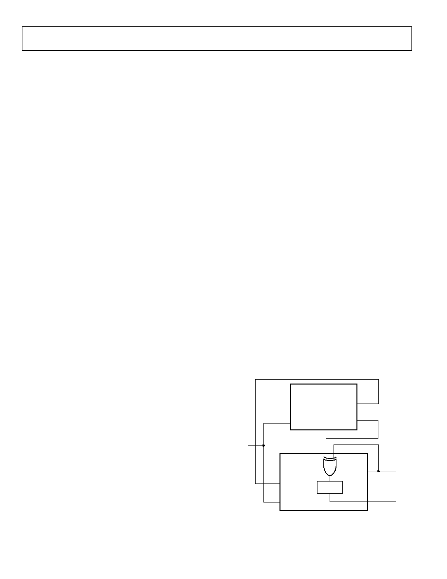
MULTICHIP SYNCHRONIZATION
The AD9511 provides a means of synchronizing two or more
AD9511s. This is not an active synchronization; it requires user
monitoring and action. The arrangement of two AD9511s to be
synchronized is shown in Figure 43.
Figure 43. Multichip Synchronization
相关PDF资料 |
PDF描述 |
|---|---|
| AD9512UCPZ-EP-R7 | IC CLOCK DIST 5OUT PLL 48LFCSP |
| AD9512UCPZ-EP | IC CLOCK DIST 5OUT PLL 48LFCSP |
| AD9513BCPZ-REEL7 | IC CLOCK DIST 3OUT PLL 32LFCSP |
| AD9514BCPZ-REEL7 | IC CLOCK DIST 3OUT PLL 32LFCSP |
| AD9515BCPZ-REEL7 | IC CLOCK DIST 2OUT PLL 32LFCSP |
相关代理商/技术参数 |
参数描述 |
|---|---|
| AD9511-VCO/PCB | 制造商:Analog Devices 功能描述:EVAL BD FOR AD9511 1.2 GHZ CLOCK DISTRIBUTION IC, PLL CORE,D - Bulk |
| AD9512 | 制造商:AD 制造商全称:Analog Devices 功能描述:800 MHz Clock Distribution IC,1.5 GHz Inputs, Dividers, Delay Adjust, Five Outputs |
| AD9512/PCB | 制造商:Analog Devices 功能描述:Evaluation Kit For 1.2 GHZ Clock Distribution IC, 1.6 GHZ Inputs, Dividers, Delay Adjust, Five Outputs 制造商:Analog Devices 功能描述:EVAL KIT FOR 1.2 GHZ CLOCK DISTRIBUTION IC, 1.6 GHZ INPUTS, - Bulk |
| AD9512/PCBZ | 功能描述:BOARD EVAL FOR AD9512 RoHS:是 类别:编程器,开发系统 >> 评估演示板和套件 系列:- 标准包装:1 系列:PSoC® 主要目的:电源管理,热管理 嵌入式:- 已用 IC / 零件:- 主要属性:- 次要属性:- 已供物品:板,CD,电源 |
| AD9512BCPZ | 功能描述:IC CLOCK DIST 5OUT PLL 48LFCSP RoHS:是 类别:集成电路 (IC) >> 时钟/计时 - 时钟发生器,PLL,频率合成器 系列:- 标准包装:2,000 系列:- 类型:PLL 时钟发生器 PLL:带旁路 输入:LVCMOS,LVPECL 输出:LVCMOS 电路数:1 比率 - 输入:输出:2:11 差分 - 输入:输出:是/无 频率 - 最大:240MHz 除法器/乘法器:是/无 电源电压:3.135 V ~ 3.465 V 工作温度:0°C ~ 70°C 安装类型:表面贴装 封装/外壳:32-LQFP 供应商设备封装:32-TQFP(7x7) 包装:带卷 (TR) |
发布紧急采购,3分钟左右您将得到回复。