- 您现在的位置:买卖IC网 > PDF目录1986 > AD9510BCPZ-REEL7 (Analog Devices Inc)IC CLOCK DIST 8OUT PLL 64LFCSP PDF资料下载
参数资料
| 型号: | AD9510BCPZ-REEL7 |
| 厂商: | Analog Devices Inc |
| 文件页数: | 25/56页 |
| 文件大小: | 0K |
| 描述: | IC CLOCK DIST 8OUT PLL 64LFCSP |
| 标准包装: | 750 |
| 类型: | 扇出缓冲器(分配),除法器 |
| PLL: | 是 |
| 输入: | 时钟 |
| 输出: | CMOS,LVDS,LVPECL |
| 电路数: | 1 |
| 比率 - 输入:输出: | 2:8 |
| 差分 - 输入:输出: | 是/是 |
| 频率 - 最大: | 1.2GHz |
| 除法器/乘法器: | 是/无 |
| 电源电压: | 3.135 V ~ 3.465 V |
| 工作温度: | -40°C ~ 85°C |
| 安装类型: | 表面贴装 |
| 封装/外壳: | 64-VFQFN 裸露焊盘,CSP |
| 供应商设备封装: | 64-LFCSP-VQ(9x9) |
| 包装: | 带卷 (TR) |
| 配用: | AD9510-VCO/PCBZ-ND - BOARD EVALUATION FOR AD9510 AD9510/PCBZ-ND - BOARD EVALUATION FOR AD9510 |
第1页第2页第3页第4页第5页第6页第7页第8页第9页第10页第11页第12页第13页第14页第15页第16页第17页第18页第19页第20页第21页第22页第23页第24页当前第25页第26页第27页第28页第29页第30页第31页第32页第33页第34页第35页第36页第37页第38页第39页第40页第41页第42页第43页第44页第45页第46页第47页第48页第49页第50页第51页第52页第53页第54页第55页第56页
Data Sheet
AD9510
Rev. B | Page 31 of 56
PLL Analog Lock Detect
An analog lock detect (ALD) signal can be selected. When ALD
is selected, the signal at the STATUS pin is either an open-drain
P-channel (Register 0x08[5:2] = 1100) or an open-drain
N-channel (Register 0x08[5:2] = 0101b).
The analog lock detect signal is true (relative to the selected
mode) with brief false pulses. These false pulses shorten as the
inputs to the PFD are nearer to coincidence and longer as they
are further from coincidence.
To extract a usable analog lock detect signal, an external resistor-
capacitor (RC) network is required to provide an analog filter
with the appropriate RC constant to allow for the discrimina-
tion of a lock condition by an external voltage comparator. A
1 k resistor in parallel with a small capacitance usually fulfills
this requirement. However, some experimentation may be
required to obtain the desired operation.
The analog lock detect function may introduce some spurious
energy into the clock outputs. It is prudent to limit the use of
the ALD when the best possible jitter/phase noise performance
is required on the clock outputs.
Loss of Reference
The AD9510 PLL can warn of a loss of reference signal at
REFIN. The loss of reference monitor internally sets a flag
called LREF. Externally, this signal can be observed in several
ways on the STATUS pin, depending on the PLL MUX control
settings in Register 0x08[5:2]. The LREF alone can be observed
as an active high signal by setting Register 0x08[5:2] = [1010] or
as an active low signal by setting Register 0x08[5:2] = [1111].
The loss of reference circuit is clocked by the signal from the
VCO, which means that there must be a VCO signal present to
detect a loss of reference.
The digital lock detect (DLD) block of the AD9510 requires a
PLL reference signal to be present in order for the digital lock
detect output to be valid. It is possible to have a digital lock
detect indication (DLD = true) that remains true even after a
loss of reference signal. For this reason, the digital lock detect
signal alone cannot be relied upon if the reference has been lost.
To combine the DLD and the LREF into a single signal at the
STATUS pin, set Register 0x08[5:2] = [1101] to obtain a signal
that is the logical OR of the loss of lock (inverse of DLD) and
the loss of reference (LREF) active high. If an active low version
of this same signal is desired, set Register 0x08[5:2] = [1110].
The reference monitor is enabled only after the DLD signal is high
for the number of PFD cycles set by the value in Register 0x07[6:5].
This delay is measured in PFD cycles. The delay ranges from 3 PFD
cycles (default) to 24 PFD cycles. When the reference goes away,
LREF goes true and the charge pump goes into tristate.
User intervention is required to take the part out of this state.
First, Register 0x07[2] = 0b must be written to disable the loss
of reference circuit, taking the charge pump out of tristate and
causing LREF to go false. A second write of Register 0x07[2] = 1
is required to reenable the loss of reference circuit.
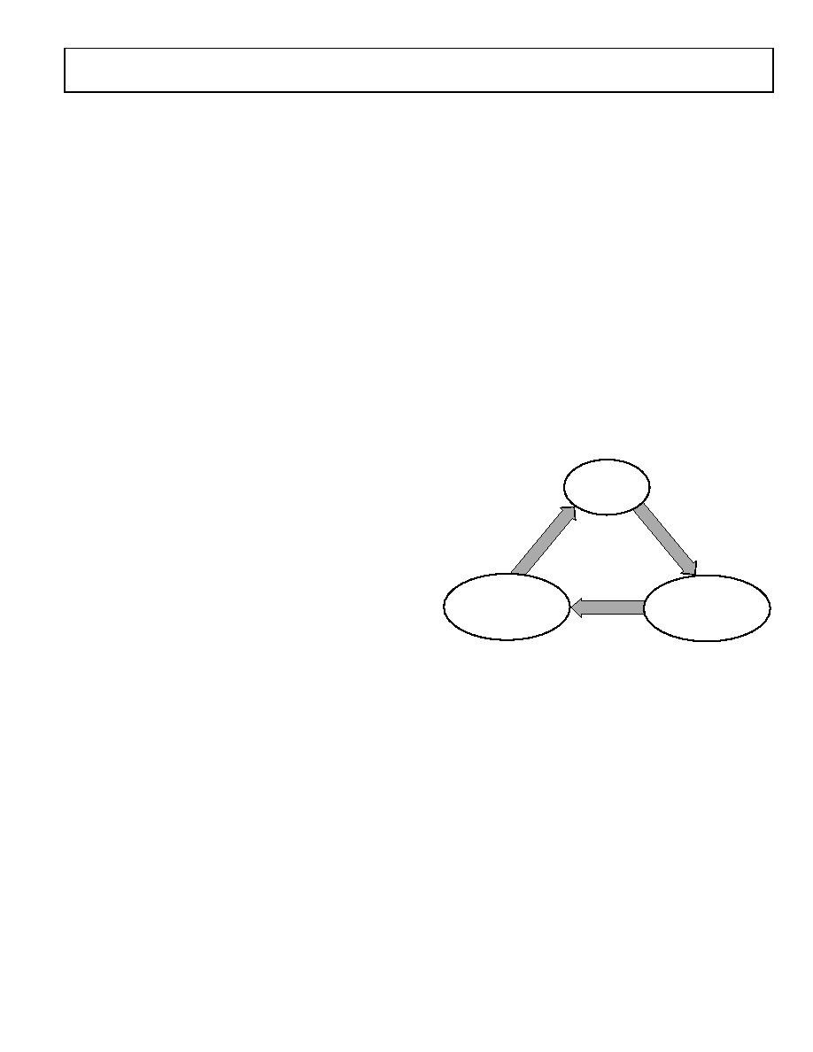
Figure 38. Loss of Reference Sequence of Events
05046-
034
PLL LOOP LOCKS
DLD GOES TRUE
LREF IS FALSE
CHECK FOR PRESENCE
OF REFERENCE.
LREF STAYS FALSE IF
REFERENCE IS DETECTED.
CHARGE PUMP
GOES INTO TRISTATE.
LREF SET TRUE.
MISSING
REFERENCE
DETECTED
n PFD CYCLES WITH
DLD TRUE
(n SET BY 0x07[6:5])
WRITE 0x07[2] = 0
LREF SET FALSE
CHARGE PUMP COMES
OUT OF TRISTATE
WRITE 0x07[2] = 1
LOR ENABLED
相关PDF资料 |
PDF描述 |
|---|---|
| AD9511BCPZ-REEL7 | IC CLOCK DIST 5OUT PLL 48LFCSP |
| AD9512UCPZ-EP-R7 | IC CLOCK DIST 5OUT PLL 48LFCSP |
| AD9512UCPZ-EP | IC CLOCK DIST 5OUT PLL 48LFCSP |
| AD9513BCPZ-REEL7 | IC CLOCK DIST 3OUT PLL 32LFCSP |
| AD9514BCPZ-REEL7 | IC CLOCK DIST 3OUT PLL 32LFCSP |
相关代理商/技术参数 |
参数描述 |
|---|---|
| AD9510-VCO/PCB | 制造商:Analog Devices 功能描述:EVAL BD FOR 1.2 GHZ CLOCK DISTRIBUTION IC, PLL CORE, DIVIDER - Bulk 制造商:Analog Devices 功能描述:IC ((NS)) |
| AD9510-VCO/PCBZ | 功能描述:BOARD EVALUATION FOR AD9510 RoHS:是 类别:编程器,开发系统 >> 评估演示板和套件 系列:- 标准包装:1 系列:PSoC® 主要目的:电源管理,热管理 嵌入式:- 已用 IC / 零件:- 主要属性:- 次要属性:- 已供物品:板,CD,电源 |
| AD9511 | 制造商:AD 制造商全称:Analog Devices 功能描述:1.2 GHz Clock Distribution IC, PLL Core, Dividers, Delay Adjust, Five Outputs |
| AD9511/PCB | 制造商:Analog Devices 功能描述:1.2 GHZ CLOCK DISTRIBUTION IC, PLL CORE,DIVIDERS, DELAY ADJUST, FIVE OUTPUTS 制造商:Analog Devices 功能描述:EVAL BD FOR AD9511 1.2 GHZ CLOCK DISTRIBUTION IC, PLL CORE,D - Bulk |
| AD9511BCPZ | 功能描述:IC CLOCK DIST 5OUT PLL 48LFCSP RoHS:是 类别:集成电路 (IC) >> 时钟/计时 - 时钟发生器,PLL,频率合成器 系列:- 标准包装:1,000 系列:Precision Edge® 类型:时钟/频率合成器 PLL:无 输入:CML,PECL 输出:CML 电路数:1 比率 - 输入:输出:2:1 差分 - 输入:输出:是/是 频率 - 最大:10.7GHz 除法器/乘法器:无/无 电源电压:2.375 V ~ 3.6 V 工作温度:-40°C ~ 85°C 安装类型:表面贴装 封装/外壳:16-VFQFN 裸露焊盘,16-MLF? 供应商设备封装:16-MLF?(3x3) 包装:带卷 (TR) 其它名称:SY58052UMGTRSY58052UMGTR-ND |
发布紧急采购,3分钟左右您将得到回复。