- 您现在的位置:买卖IC网 > PDF目录1194 > ADP1043AFB100EVALZ (Analog Devices Inc)BOARD EVALUATION ADP1043A 100W PDF资料下载
参数资料
| 型号: | ADP1043AFB100EVALZ |
| 厂商: | Analog Devices Inc |
| 文件页数: | 65/72页 |
| 文件大小: | 0K |
| 描述: | BOARD EVALUATION ADP1043A 100W |
| 标准包装: | 1 |
| 主要目的: | 电源管理,电源监控器/跟踪器/序列发生器 |
| 已用 IC / 零件: | ADP1043A |
| 主要属性: | * |
| 次要属性: | * |
| 已供物品: | 板 |
第1页第2页第3页第4页第5页第6页第7页第8页第9页第10页第11页第12页第13页第14页第15页第16页第17页第18页第19页第20页第21页第22页第23页第24页第25页第26页第27页第28页第29页第30页第31页第32页第33页第34页第35页第36页第37页第38页第39页第40页第41页第42页第43页第44页第45页第46页第47页第48页第49页第50页第51页第52页第53页第54页第55页第56页第57页第58页第59页第60页第61页第62页第63页第64页当前第65页第66页第67页第68页第69页第70页第71页第72页
�� ��
��
��ADP1043A�
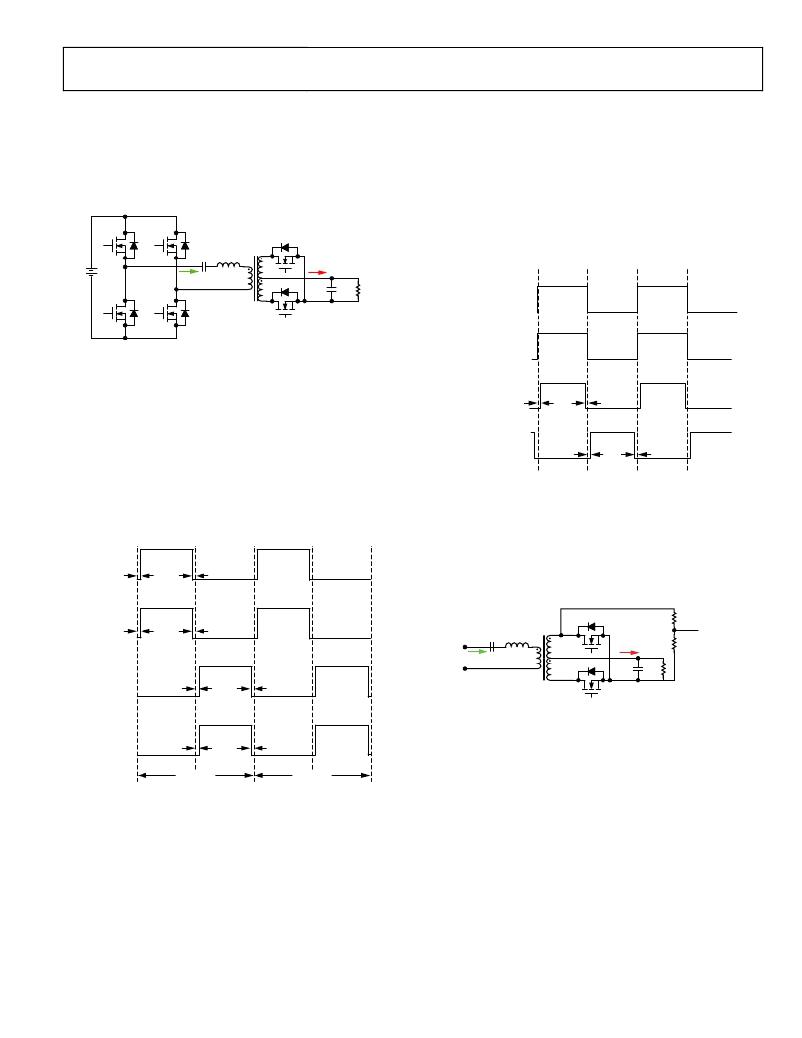
�RESONANT� MODE� OPERATION�
�The� ADP1043A� supports� control� of� a� resonant� converter.�
�Resonant� converters� are� an� alternative� to� traditional� fixed�
�frequency� converters.� They� offer� high� switching� frequency,�
�small� size,� and� high� efficiency.� Figure� 38� illustrates� a� widely�
�used� series� resonant� converter.�
�SYNCHRONOUS� RECTIFICATION� IN� RESONANT�
�MODE�
�Control� of� the� synchronous� rectifiers� in� a� resonant� controller� is�
�a� complicated� issue.� The� ADP1043A� ACSNS� comparator� can� be�
�used� to� control� the� SR� signals.� In� resonant� mode� operation,� the�
�Q� A�
�Q� C�
�SR2�
�SR1� output� is� driven� by� the� rising� edge� of� the� ACSNS� comparator,�
�and� the� SR2� output� is� driven� by� the� falling� edge� of� the� comparator,�
�C� R�
�L� R�
�I� O�
��Q� D�
�Q� B�
�I� R�
�SR1�
�C� O�
�R� L�
�V� DS� (SR2)�
�Figure� 38.� Series� Resonant� Converter�
�RESONANT� MODE� ENABLE�
�ACSNS�
�To� enable� the� ADP1043A� to� control� a� resonant� switching� con-�
�SYNC� RECT� 1� (SR1)�
�Δ� t� 9�
�Δ� t� 10�
�verter,� Register� 0x40� must� be� set� to� a� value� of� 0x3F.� In� resonant�
�mode,� the� PWM� outputs� have� a� fixed� duty� cycle� with� variable�
�frequency.�
�SYNC� RECT� 2� (SR2)�
�Δ� t� 11�
�Δ� t� 12�
�PWM� TIMING� IN� RESONANT� MODE�
�With� variable� frequency� control,� OUTA� and� OUTB� can� only� be�
�high� during� the� first� half� of� the� switching� cycle� (t� A� to� t� B� ),� whereas�
�OUTC� and� OUTD� can� only� be� high� during� the� second� half� of�
��t� D� t� E� t� F�
�Figure� 40.� SR1� and� SR2� PWM� Timing� Diagram� in� Resonant� Mode�
�Following� is� an� example� of� how� the� ADP1043A� can� be� used�
�in� a� series� resonant� topology� and� also� achieve� control� of� the�
�synchronous� rectifiers.� The� V� DS� voltage� of� SR2� can� be� used� to�
�PWM1� (OUTA)�
�Δ� t� 1�
�Δ� t� 2�
�control� the� SR� signals.� The� ACSNS� pin� is� connected� to� the�
�divided-down� SR2� V� DS� voltage.� This� provides� the� timing�
�information� for� both� synchronous� rectifiers� (see� Figure� 41).�
�PWM2� (OUTB)�
�Δ� t� 3�
�Δ� t� 4�
�C� R�
�L� R�
�SR2�
�R� 1�
�ACSNS�
�I� O�
�R� 2�
�PWM3� (OUTC)�
�Δ� t� 5�
�Δ� t� 6�
�I� R�
�SR1�
�C� O�
�R� L�
�Figure� 41.� Resonant� Synchronous� Rectifier� Control� Circuit�
�PWM4� (OUTD)�
�Δ� t� 7�
�Δ� t� 8�
�After� the� timing� information� is� obtained,� SR1� is� driven� by� the�
�rising� edge� of� the� ACSNS� comparator,� and� SR2� is� driven� by� the�
�falling� edge� of� the� comparator,� as� shown� in� Figure� 40.� In� this�
�t� PERIOD�
�t� PERIOD�
�way,� it� is� possible� to� achieve� synchronous� rectification.� Turn-on�
�t� A�
�t� B�
�t� C�
�and� turn-off� delays� can� be� programmed� for� the� SR1� and� SR2�
�Figure� 39.� OUTA,� OUTB,� OUTC,� and� OUTD� PWM� Timing� Diagram�
�in� Resonant� Mode�
�signals� individually.�
�This� example� is� not� the� only� way� to� control� the� SR� signals.� If� the�
�user� has� another� method� to� control� the� SR� signals,� this� method�
�can� be� used� to� connect� to� the� ACSNS� input� instead� of� the� V� DS�
�voltage� of� SR2.�
�Rev.� 0� |� Page� 65� of� 72�
�相关PDF资料 |
PDF描述 |
|---|---|
| ADP1046-100-EVALZ | BOARD EVAL FOR ADP1046-100 |
| ADP1048-600-EVALZ | BOARD EVAL ADP1048-600 |
| ADP190CB-EVALZ | BOARD EVAL ADP190 |
| ADP191CB-EVALZ | EVAL BOARD FOR ADP191 |
| ADP194CB-EVALZ | BOARD EVAL FOR ADP194ACBZ |
相关代理商/技术参数 |
参数描述 |
|---|---|
| ADP1043AIF300EVALZ | 制造商:Analog Devices 功能描述:ADP1043A 300W EVALUATION BOARD - Boxed Product (Development Kits) |
| ADP1043A-USB-Z | 功能描述:EVAL BOARD DIG POWER SUPPLY RoHS:是 类别:编程器,开发系统 >> 配件 系列:- 产品培训模块:Lead (SnPb) Finish for COTS Obsolescence Mitigation Program RoHS指令信息:IButton RoHS Compliance Plan 标准包装:1 系列:- 附件类型:USB 至 1-Wire? RJ11 适配器 适用于相关产品:1-Wire? 设备 产品目录页面:1429 (CN2011-ZH PDF) |
| ADP1043-EVALZ | 制造商:Analog Devices 功能描述:EVALUATION BOARDS - Bulk |
| ADP1043FB100-EVALZ | 制造商:Analog Devices 功能描述:ADP1043 100W EVALUATION BOARD |
| ADP1045ACPZ-RL | 制造商:Analog Devices 功能描述: |
发布紧急采购,3分钟左右您将得到回复。