- 您现在的位置:买卖IC网 > PDF目录1908 > COP8CCR9KMT8 (National Semiconductor)IC MCU EEPROM 8BIT 32K 56-TSSOP PDF资料下载
参数资料
| 型号: | COP8CCR9KMT8 |
| 厂商: | National Semiconductor |
| 文件页数: | 44/111页 |
| 文件大小: | 0K |
| 描述: | IC MCU EEPROM 8BIT 32K 56-TSSOP |
| 标准包装: | 34 |
| 系列: | COP8™ 8C |
| 核心处理器: | COP8 |
| 芯体尺寸: | 8-位 |
| 速度: | 20MHz |
| 连通性: | Microwire/Plus(SPI),UART/USART |
| 外围设备: | 欠压检测/复位,POR,PWM,WDT |
| 输入/输出数: | 49 |
| 程序存储器容量: | 32KB(32K x 8) |
| 程序存储器类型: | 闪存 |
| RAM 容量: | 1K x 8 |
| 电压 - 电源 (Vcc/Vdd): | 2.7 V ~ 5.5 V |
| 数据转换器: | A/D 16x10b |
| 振荡器型: | 内部 |
| 工作温度: | -40°C ~ 85°C |
| 封装/外壳: | 56-TFSOP(0.240",6.10mm 宽) |
| 包装: | 管件 |
| 其它名称: | *COP8CCR9KMT8 |
第1页第2页第3页第4页第5页第6页第7页第8页第9页第10页第11页第12页第13页第14页第15页第16页第17页第18页第19页第20页第21页第22页第23页第24页第25页第26页第27页第28页第29页第30页第31页第32页第33页第34页第35页第36页第37页第38页第39页第40页第41页第42页第43页当前第44页第45页第46页第47页第48页第49页第50页第51页第52页第53页第54页第55页第56页第57页第58页第59页第60页第61页第62页第63页第64页第65页第66页第67页第68页第69页第70页第71页第72页第73页第74页第75页第76页第77页第78页第79页第80页第81页第82页第83页第84页第85页第86页第87页第88页第89页第90页第91页第92页第93页第94页第95页第96页第97页第98页第99页第100页第101页第102页第103页第104页第105页第106页第107页第108页第109页第110页第111页
SNOS535I – OCTOBER 2000 – REVISED MARCH 2013
The method to force this condition is to drive the G6 pin to high voltage (2 x VCC) and activate Reset. The
high voltage condition on G6 must not be applied before VCC is valid and stable, and must be held for at
least 3 instruction cycles longer than Reset is active. This special condition will bypass checking the state
of the Flex bit in the Option Register and will start execution from location 0000 in the Boot ROM. In this
state, the user can input the appropriate commands, using MICROWIRE/PLUS, to erase the flash
program memory and reprogram it. If the device is subsequently reset before the Flex bit has been erased
by specific Page Erase or Mass Erase ISP commands, execution will start from location 0000 in the Flash
program memory. The high voltage (2 x VCC) on G6 will not erase either the Flex or the Security bit in the
Option Register. The Security bit, if set, can only be erased by a Mass Erase of the entire contents of the
Flash Memory unless under the control of User ISP routines in the Application Program.
While the G6 pin is at high voltage, the Load Clock will be output onto G5, which will look like an SK clock
to the MICROWIRE/PLUS routine executing in slave mode. However, when G6 is at high voltage, the G6
input will also look like a logic 1. The MICROWIRE/PLUS routine in Boot ROM monitors the G6 input,
waits for it to go low, debounces it, and then enables the ISP routine. CAUTION: The Load clock on G5
could be in conflict with the user's external SK. It is up to the user to resolve this conflict, as this condition
is considered a minor issue that's only encountered during software development. The user should also
be cautious of the high voltage applied to the G6 pin. This high voltage could damage other
circuitry connected to the G6 pin (e.g. the parallel port of a PC). The user may wish to disconnect
other circuitry while G6 is connected to the high voltage.
VCC must be valid and stable before high voltage is applied to G6.
The correct sequence to be used to force execution from Boot ROM is :
1. Disconnect G6 from the source of data for MICROWIRE/PLUS ISP.
2. Apply VCC to the device.
3. Pull RESET Low.
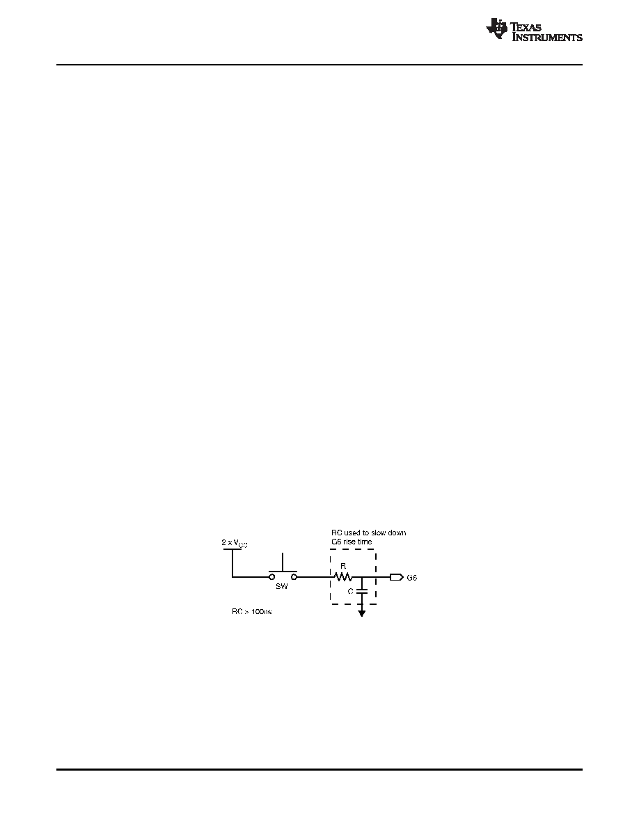
4. After VCC is valid and stable, connect a voltage between 2 x VCC and VCC+7V to the G6 pin. Ensure
that the rise time of the high voltage on G6 is slower than the minimum in the Electrical Specifications.
Figure 5-8 shows a possible circuit dliagram for implementing the 2 x VCC. Be aware of the typical input
current on the G6 pin when the high voltage is applied. The resistor used in the RC network, and the
high voltage used, should be chosen to keep the high voltage at the G6 pin between 2 x VCC and
VCC+7V.
5. Pull RESET High.
6. After a delay of at least three instruction cycles, remove the high voltage from G6.
Figure 5-8. Circuit Diagram for Implementing the 2 x VCC
5.10.6 RETURN TO FLASH MEMORY WITHOUT HARDWARE RESET
After programming the entire program memory, including options, it is necessary to exit the Boot ROM and
return to the flash program memory for program execution. Upon receipt and completion of the EXIT
command through the MICROWIRE/PLUS ISP, the ISP code will reset the part and begin execution from
the flash program memory as described in the Reset section. This assumes that the FLEX bit in the
Option register was programmed to 1.
38
Functional Description
Copyright 2000–2013, Texas Instruments Incorporated
相关PDF资料 |
PDF描述 |
|---|---|
| COP8SAA716M8/NOPB | IC MCU OTP 8BIT 1K 16-SOIC |
| CP2101-GMR | IC CTRLR BRIDGE USB-UART 28MLP |
| CP2103-GMR | IC CTRLR BRIDGE USB-UART 28MLP |
| CP2104-F03-GM | IC SGL USB-TO-UART BRIDGE 24QFN |
| CP2105-F01-GM | IC SGL USB-DL UART BRIDGE 24QFN |
相关代理商/技术参数 |
参数描述 |
|---|---|
| COP8CCR9LVA7 | 功能描述:8位微控制器 -MCU RoHS:否 制造商:Silicon Labs 核心:8051 处理器系列:C8051F39x 数据总线宽度:8 bit 最大时钟频率:50 MHz 程序存储器大小:16 KB 数据 RAM 大小:1 KB 片上 ADC:Yes 工作电源电压:1.8 V to 3.6 V 工作温度范围:- 40 C to + 105 C 封装 / 箱体:QFN-20 安装风格:SMD/SMT |
| COP8CCR9LVA7/63 | 制造商:Texas Instruments 功能描述: |
| COP8CCR9LVA7/63SN | 功能描述:闪存 RoHS:否 制造商:ON Semiconductor 数据总线宽度:1 bit 存储类型:Flash 存储容量:2 MB 结构:256 K x 8 定时类型: 接口类型:SPI 访问时间: 电源电压-最大:3.6 V 电源电压-最小:2.3 V 最大工作电流:15 mA 工作温度:- 40 C to + 85 C 安装风格:SMD/SMT 封装 / 箱体: 封装:Reel |
| COP8CCR9LVA7/NOPB | 功能描述:8位微控制器 -MCU RoHS:否 制造商:Silicon Labs 核心:8051 处理器系列:C8051F39x 数据总线宽度:8 bit 最大时钟频率:50 MHz 程序存储器大小:16 KB 数据 RAM 大小:1 KB 片上 ADC:Yes 工作电源电压:1.8 V to 3.6 V 工作温度范围:- 40 C to + 105 C 封装 / 箱体:QFN-20 安装风格:SMD/SMT |
| COP8CCR9LVA763SN | 制造商:National Semiconductor 功能描述:MCU 8-bit COP8 CISC 32KB Flash 5V 68-Pin PLCC |
发布紧急采购,3分钟左右您将得到回复。