- 您现在的位置:买卖IC网 > PDF目录170654 > DAC5688IRGCTG4 (TEXAS INSTRUMENTS INC) PARALLEL, WORD INPUT LOADING, 0.0104 us SETTLING TIME, 16-BIT DAC, PQCC64 PDF资料下载
参数资料
| 型号: | DAC5688IRGCTG4 |
| 厂商: | TEXAS INSTRUMENTS INC |
| 元件分类: | DAC |
| 英文描述: | PARALLEL, WORD INPUT LOADING, 0.0104 us SETTLING TIME, 16-BIT DAC, PQCC64 |
| 封装: | 9 X 9 MM, GREEN, PLASTIC, VQFN-64 |
| 文件页数: | 23/56页 |
| 文件大小: | 1321K |
| 代理商: | DAC5688IRGCTG4 |
第1页第2页第3页第4页第5页第6页第7页第8页第9页第10页第11页第12页第13页第14页第15页第16页第17页第18页第19页第20页第21页第22页当前第23页第24页第25页第26页第27页第28页第29页第30页第31页第32页第33页第34页第35页第36页第37页第38页第39页第40页第41页第42页第43页第44页第45页第46页第47页第48页第49页第50页第51页第52页第53页第54页第55页第56页
www.ti.com
SLLS880C – DECEMBER 2007 – REVISED AUGUST 2010
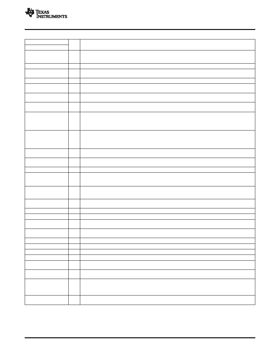
PIN FUNCTIONS
PIN
I/O
DESCRIPTION
NAME
NO.
51, 54,
AVDD
55, 59,
I
Analog supply voltage. (3.3V)
62
BIASJ
57
O
Full-scale output current bias. For 20mA full-scale output current, connect a 960
resistor to GND.
With the clock multiplier PLL enabled, CLK2 provides lower frequency reference clock. If the PLL is disabled, CLK2
CLK2
2
I
directly provides clock for DAC up to 800 MHz.
CLK2C
3
I
Complementary CLK2 input.
In Dual Clock Modes, provides lower frequency input clock (CLK1). Optionally provides clock (CLKO) output for data
CLKO_CLK1
25
I/O
bus. Internal pull-down.
Complementary CLK1 signal if configured as a differential input. In PLL mode, optionally outputs PLL lock status. Internal
LOCK_ CLK1C
26
I/O
pull-down.
Internal clock buffer supply voltage. (1.8V)
CLKVDD
1
I
It is recommended to isolate this supply from DVDD.
A-Channel Data Bits 0 through 15.
DA15 is most significant data bit (MSB) – pin 7
7, 8,
DA[15..0]
I
11–24
DA0 is least significant data bit (LSB) – pin 24
Internal pull-down. The order of bus can be reversed via CONFIG4 reva bit.
B-Channel Data Bits 0 through 15.
DB15 is most significant data bit (MSB) – pin 43
40–43,
DB[15..0]
I
27–38
DB0 is least significant data bit (LSB) – pin 27
Internal pull-down. The order of bus can be reversed via CONFIG4 revb bit.
10, 39,
Digital supply voltage. (1.8V)
DVDD
I
50, 63
For best performance it is recommended to isolate pins 10 and 39 from all other 1.8V supplies.
Used as external reference input when internal reference is disabled (i.e., EXTLO connected to AVDD). Used as internal
EXTIO
56
I/O
reference output when EXTLO = GND, requires a 0.1mF decoupling capacitor to GND when used as reference output
EXTLO
58
O
Connect to GND for internal reference, or AVDD for external reference.
4,
GND
I
Pin 4 and the Thermal Pad located on the bottom of the QFN package is ground for AVDD, DVDD and IOVDD supplies.
Thermal
Pad
A-Channel DAC current output. An offset binary data pattern of 0x0000 at the DAC input results in a full scale current
IOUTA1
52
O
sink and the least positive voltage on the IOUTA1 pin. Similarly, a 0xFFFF data input results in a 0 mA current sink and
the most positive voltage on the IOUTA1 pin. In single DAC mode, outputs appear on the IOUTA1/A2 pair only.
A-Channel DAC complementary current output. The IOUTA2 has the opposite behavior of the IOUTA1 described above.
IOUTA2
53
O
An input data value of 0x0000 results in a 0mA sink and the most positive voltage on the IOUTA2 pin.
IOUTB1
61
O
B-Channel DAC current output. Refer to IOUTA1 description above.
IOUTB2
60
O
B-Channel DAC complementary current output. Refer to IOUTA2 description above.
3.3V supply voltage for all digital I/O. Note: This supply input should remain at 3.3V regardless of the 1.8V or 3.3V
IOVDD
9
I
selectable digital input switching thresholds via CONFIG26 io_1p8_3p3.
PLL loop filter connection. If not using the clock multiplying PLL, leave the LPF pin open. Set PLL_sleep and clear
LPF
64
I
PLL_ena control bits for reduced power dissipation.
SYNC
5
I
Optional SYNC input for internal clock dividers, FIFO, NCO and QMC blocks. Internal pull-down.
RESETB
49
I
Resets the chip when low. Internal pull-up.
SCLK
47
I
Serial interface clock. Internal pull-down.
SDENB
48
I
Active low serial data enable, always an input to the DAC5688. Internal pull-up.
Bi-directional serial data in 3-pin mode (default). In 4-pin interface mode (CONFIG5 sif4), the SDIO pin is an input only.
SDIO
46
I/O
Internal pull-down.
Uni-directional serial interface data in 4-pin mode (CONFIG5 sif4). The SDO pin is tri-stated in 3-pin interface mode
SDO
45
O
(default). Internal pull-down.
Transmit enable input. Internal pull-down. TXENABLE has two purposes. In all modes, TXENABLE must be high for the
DATA to the DAC to be enabled. When TXENABLE is low, the digital logic section is forced to all 0, and any input data is
TXENABLE
6
I
ignored. In interleaved data mode, TXENABLE can be used to synchronize the data to channels A and B. The first
A-channels sample should be aligned with the rising edge of TXENABLE.
Digital supply voltage. (1.8V) This supply pin is also used for factory fuse programming. Connect to DVDD pins for
VFUSE
44
I
normal operation.
Copyright 2007–2010, Texas Instruments Incorporated
3
Product Folder Link(s): DAC5688
相关PDF资料 |
PDF描述 |
|---|---|
| DAC702LH | PARALLEL, WORD INPUT LOADING, 4 us SETTLING TIME, 16-BIT DAC, CDIP24 |
| DAC7545KUG4 | PARALLEL, WORD INPUT LOADING, 2 us SETTLING TIME, 12-BIT DAC, PDSO20 |
| DAC7545JP | PARALLEL, WORD INPUT LOADING, 2 us SETTLING TIME, 12-BIT DAC, PDIP20 |
| DAC7545KP | PARALLEL, WORD INPUT LOADING, 2 us SETTLING TIME, 12-BIT DAC, PDIP20 |
| DAC7554IDGSR | SERIAL INPUT LOADING, 5 us SETTLING TIME, 12-BIT DAC, PDSO10 |
相关代理商/技术参数 |
参数描述 |
|---|---|
| DAC5689 | 制造商:TI 制造商全称:Texas Instruments 功能描述:16-BIT 800 MSPS 2x-8x INTERPOLATING DUAL-CHANNEL DIGITAL-TO-ANALOG CONVERTER (DAC) |
| DAC5689EVM | 功能描述:数据转换 IC 开发工具 DAC5689 Eval Mod RoHS:否 制造商:Texas Instruments 产品:Demonstration Kits 类型:ADC 工具用于评估:ADS130E08 接口类型:SPI 工作电源电压:- 6 V to + 6 V |
| DAC5689IRGCR | 功能描述:数模转换器- DAC 16B,800MSPS 2x-8x Int Dual-Channel DAC RoHS:否 制造商:Texas Instruments 转换器数量:1 DAC 输出端数量:1 转换速率:2 MSPs 分辨率:16 bit 接口类型:QSPI, SPI, Serial (3-Wire, Microwire) 稳定时间:1 us 最大工作温度:+ 85 C 安装风格:SMD/SMT 封装 / 箱体:SOIC-14 封装:Tube |
| DAC5689IRGCT | 功能描述:数模转换器- DAC 16B,800MSPS 2x-8x Int Dual-Channel DAC RoHS:否 制造商:Texas Instruments 转换器数量:1 DAC 输出端数量:1 转换速率:2 MSPs 分辨率:16 bit 接口类型:QSPI, SPI, Serial (3-Wire, Microwire) 稳定时间:1 us 最大工作温度:+ 85 C 安装风格:SMD/SMT 封装 / 箱体:SOIC-14 封装:Tube |
| DAC56P | 制造商:TI 制造商全称:Texas Instruments 功能描述:Monolithic 16-Bit Resolution DIGITAL-TO-ANALOG CONVERTER |
发布紧急采购,3分钟左右您将得到回复。