- 您现在的位置:买卖IC网 > PDF目录170654 > DAC5688IRGCTG4 (TEXAS INSTRUMENTS INC) PARALLEL, WORD INPUT LOADING, 0.0104 us SETTLING TIME, 16-BIT DAC, PQCC64 PDF资料下载
参数资料
| 型号: | DAC5688IRGCTG4 |
| 厂商: | TEXAS INSTRUMENTS INC |
| 元件分类: | DAC |
| 英文描述: | PARALLEL, WORD INPUT LOADING, 0.0104 us SETTLING TIME, 16-BIT DAC, PQCC64 |
| 封装: | 9 X 9 MM, GREEN, PLASTIC, VQFN-64 |
| 文件页数: | 27/56页 |
| 文件大小: | 1321K |
| 代理商: | DAC5688IRGCTG4 |
第1页第2页第3页第4页第5页第6页第7页第8页第9页第10页第11页第12页第13页第14页第15页第16页第17页第18页第19页第20页第21页第22页第23页第24页第25页第26页当前第27页第28页第29页第30页第31页第32页第33页第34页第35页第36页第37页第38页第39页第40页第41页第42页第43页第44页第45页第46页第47页第48页第49页第50页第51页第52页第53页第54页第55页第56页
CLK 2
CLK 1
D < t_align
DA [0 : 15 ]
DB [0 : 15 ]
t s
th
(only in dual synchronous clock mode)
www.ti.com
SLLS880C – DECEMBER 2007 – REVISED AUGUST 2010
CLOCK MODES
The DAC5688 supports several different clocking modes for generating the internal clocks for the logic and DAC.
The clocking modes are selected by programming the register bits below and summarized in Table 5.
Register
Control Bits
CONFIG1
synchr_clkin
CONFIG2
clk1_in_ena, clk1c_in_ena, diffclk_ena
CONFIG26
PLL_ena
Table 5. Summary of Clock Modes and Options
CLKO_
Programming Bits
CLK1
synchr_clkin
clk1_in_en
clk1c_in_ena
diffclk_ena
PLL_ena
Clocking Mode
Option
I/O
Dual Synchronous Clock Mode
Diff. CLK1
Input
1
0
S/E CLK1
Input
1
X
0
Dual Clock Mode
Diff. CLK1
Input
0
1
0
S/E CLK1
Input
0
1
X
0
External Clock Mode
CLKO
Output
0
X
0
PLL Clock Mode
Diff. CLK1
Input
0
1
S/E CLK1
Input
0
1
X
0
1
CLKO
Output
0
X
0
1
DUAL SYNCHRONOUS CLOCK MODE
In DUAL SYNCHRONOUS CLOCK MODE, the user provides the CLK2/C clock signal at the DAC sample rate
and also provides a divided down CLK1 at the input data rate. The CLK1 signal can be differential or
single-ended. Refer to Figure 16 for the timing diagram. In this mode the relationship between CLK2 and CLK1
(t_align) is critical and used as a synchronizing mechanism for the internal logic. This facilitates multi-DAC
synchronization by using dual external clock inputs CLK1 and CLK2 while FIFO data is always written and read
from location zero. It is highly recommended that a clock synchronizer device such as the CDCM7005 provide
both CLK2/C and CLK1/C inputs. Although CLK1 could be single-ended it is recommended to use a differential
clock to ensure proper skews between the two clock inputs.
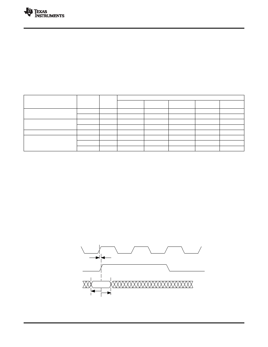
DUAL CLOCK MODE
In DUAL CLOCK MODE, the user provides the CLK2/C clock signal at the DAC sample rate and also provides a
divided down CLK1 at the input data rate. The CLK1 signal can be differential or single-ended. Refer to Figure 32
for the timing diagram. Unlike the DUAL SYNCHRONOUS CLOCK MODE, the t_align parameter is not critical
because these clocks are not used as a synchronizing mechanism for the internal logic and the FIFO is used as
an elastic buffer for the data. Synchronizing in this mode is provided by separate control inputs.
Figure 32. DUAL (SYNCHRONOUS) CLOCK MODE Timing Diagram
Copyright 2007–2010, Texas Instruments Incorporated
33
Product Folder Link(s): DAC5688
相关PDF资料 |
PDF描述 |
|---|---|
| DAC702LH | PARALLEL, WORD INPUT LOADING, 4 us SETTLING TIME, 16-BIT DAC, CDIP24 |
| DAC7545KUG4 | PARALLEL, WORD INPUT LOADING, 2 us SETTLING TIME, 12-BIT DAC, PDSO20 |
| DAC7545JP | PARALLEL, WORD INPUT LOADING, 2 us SETTLING TIME, 12-BIT DAC, PDIP20 |
| DAC7545KP | PARALLEL, WORD INPUT LOADING, 2 us SETTLING TIME, 12-BIT DAC, PDIP20 |
| DAC7554IDGSR | SERIAL INPUT LOADING, 5 us SETTLING TIME, 12-BIT DAC, PDSO10 |
相关代理商/技术参数 |
参数描述 |
|---|---|
| DAC5689 | 制造商:TI 制造商全称:Texas Instruments 功能描述:16-BIT 800 MSPS 2x-8x INTERPOLATING DUAL-CHANNEL DIGITAL-TO-ANALOG CONVERTER (DAC) |
| DAC5689EVM | 功能描述:数据转换 IC 开发工具 DAC5689 Eval Mod RoHS:否 制造商:Texas Instruments 产品:Demonstration Kits 类型:ADC 工具用于评估:ADS130E08 接口类型:SPI 工作电源电压:- 6 V to + 6 V |
| DAC5689IRGCR | 功能描述:数模转换器- DAC 16B,800MSPS 2x-8x Int Dual-Channel DAC RoHS:否 制造商:Texas Instruments 转换器数量:1 DAC 输出端数量:1 转换速率:2 MSPs 分辨率:16 bit 接口类型:QSPI, SPI, Serial (3-Wire, Microwire) 稳定时间:1 us 最大工作温度:+ 85 C 安装风格:SMD/SMT 封装 / 箱体:SOIC-14 封装:Tube |
| DAC5689IRGCT | 功能描述:数模转换器- DAC 16B,800MSPS 2x-8x Int Dual-Channel DAC RoHS:否 制造商:Texas Instruments 转换器数量:1 DAC 输出端数量:1 转换速率:2 MSPs 分辨率:16 bit 接口类型:QSPI, SPI, Serial (3-Wire, Microwire) 稳定时间:1 us 最大工作温度:+ 85 C 安装风格:SMD/SMT 封装 / 箱体:SOIC-14 封装:Tube |
| DAC56P | 制造商:TI 制造商全称:Texas Instruments 功能描述:Monolithic 16-Bit Resolution DIGITAL-TO-ANALOG CONVERTER |
发布紧急采购,3分钟左右您将得到回复。