- 您现在的位置:买卖IC网 > PDF目录170654 > DAC5688IRGCTG4 (TEXAS INSTRUMENTS INC) PARALLEL, WORD INPUT LOADING, 0.0104 us SETTLING TIME, 16-BIT DAC, PQCC64 PDF资料下载
参数资料
| 型号: | DAC5688IRGCTG4 |
| 厂商: | TEXAS INSTRUMENTS INC |
| 元件分类: | DAC |
| 英文描述: | PARALLEL, WORD INPUT LOADING, 0.0104 us SETTLING TIME, 16-BIT DAC, PQCC64 |
| 封装: | 9 X 9 MM, GREEN, PLASTIC, VQFN-64 |
| 文件页数: | 35/56页 |
| 文件大小: | 1321K |
| 代理商: | DAC5688IRGCTG4 |
第1页第2页第3页第4页第5页第6页第7页第8页第9页第10页第11页第12页第13页第14页第15页第16页第17页第18页第19页第20页第21页第22页第23页第24页第25页第26页第27页第28页第29页第30页第31页第32页第33页第34页当前第35页第36页第37页第38页第39页第40页第41页第42页第43页第44页第45页第46页第47页第48页第49页第50页第51页第52页第53页第54页第55页第56页
SLLS880C – DECEMBER 2007 – REVISED AUGUST 2010
www.ti.com
The full-scale output current is set using external resistor RBIAS in combination with an on-chip bandgap voltage
reference source (+1.2 V) and control amplifier. Current IBIAS through resistor RBIAS is mirrored internally to
provide a maximum full-scale output current equal to 16 times IBIAS.
The relation between IOUT1 and IOUT2 can be expressed as:
IOUT1 = – IOUTFS – IOUT2
We will denote current flowing into a node as – current and current flowing out of a node as + current. Since the
output stage is a current sink the current can only flow from AVDD into the IOUT1 and IOUT2 pins. The output
current flow in each pin driving a resistive load can be expressed as:
IOUT1 = IOUTFS × (65536 – CODE) / 65536
IOUT2 = IOUTFS × CODE / 65536
where CODE is the decimal representation of the DAC data input word.
For the case where IOUT1 and IOUT2 drive resistor loads RL directly, this translates into single ended voltages
at IOUT1 and IOUT2:
VOUT1 = AVDD – | IOUT1 | × RL
VOUT2 = AVDD – | IOUT2 | × RL
Assuming that the data is full scale (65536 in offset binary notation) and the RL is 25 , the differential voltage
between pins IOUT1 and IOUT2 can be expressed as:
VOUT1 = AVDD – | –0mA | × 25
= 3.3 V
VOUT2 = AVDD – | –20mA | × 25
= 2.8 V
VDIFF = VOUT1 – VOUT2 = 0.5V
Note that care should be taken not to exceed the compliance voltages at node IOUT1 and IOUT2, which would
lead to increased signal distortion.
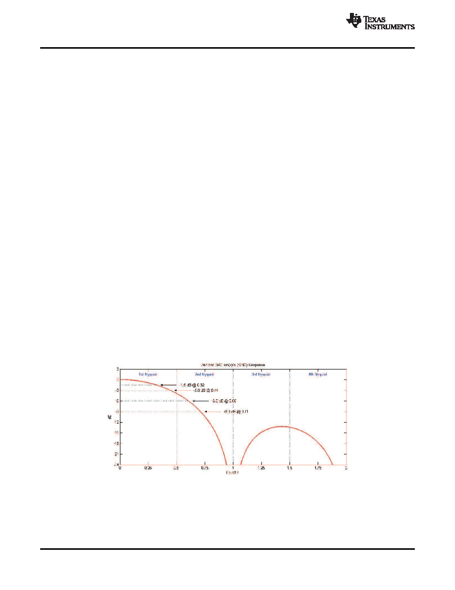
DAC OUTPUT SINC RESPONSE
Due to sampled nature of a high-speed DAC’s, the well known sin(x)/x (or SINC) response can significantly
attenuate higher frequency output signals. Refer to Figure 44 which shows the unitized SINC attenuation roll-off
with respect to the final DAC sample rate in 4 Nyquist zones. For example, if the final DAC sample rate FS = 1.0
GSPS, then a tone at 440MHz will be attenuated by 3.0dB. Although the SINC response can create challenges
in frequency planning, one side benefit is the natural attenuation of Nyquist images. The increased over-sampling
ratio of the input data provided by the DAC5688’s 2x, 4x and 8x digital interpolation modes improve the SINC
roll-off (droop) within the original signal’s band of interest.
Figure 44. Unitized DAC sin(x)/x (SINC) Response
40
Copyright 2007–2010, Texas Instruments Incorporated
Product Folder Link(s): DAC5688
相关PDF资料 |
PDF描述 |
|---|---|
| DAC702LH | PARALLEL, WORD INPUT LOADING, 4 us SETTLING TIME, 16-BIT DAC, CDIP24 |
| DAC7545KUG4 | PARALLEL, WORD INPUT LOADING, 2 us SETTLING TIME, 12-BIT DAC, PDSO20 |
| DAC7545JP | PARALLEL, WORD INPUT LOADING, 2 us SETTLING TIME, 12-BIT DAC, PDIP20 |
| DAC7545KP | PARALLEL, WORD INPUT LOADING, 2 us SETTLING TIME, 12-BIT DAC, PDIP20 |
| DAC7554IDGSR | SERIAL INPUT LOADING, 5 us SETTLING TIME, 12-BIT DAC, PDSO10 |
相关代理商/技术参数 |
参数描述 |
|---|---|
| DAC5689 | 制造商:TI 制造商全称:Texas Instruments 功能描述:16-BIT 800 MSPS 2x-8x INTERPOLATING DUAL-CHANNEL DIGITAL-TO-ANALOG CONVERTER (DAC) |
| DAC5689EVM | 功能描述:数据转换 IC 开发工具 DAC5689 Eval Mod RoHS:否 制造商:Texas Instruments 产品:Demonstration Kits 类型:ADC 工具用于评估:ADS130E08 接口类型:SPI 工作电源电压:- 6 V to + 6 V |
| DAC5689IRGCR | 功能描述:数模转换器- DAC 16B,800MSPS 2x-8x Int Dual-Channel DAC RoHS:否 制造商:Texas Instruments 转换器数量:1 DAC 输出端数量:1 转换速率:2 MSPs 分辨率:16 bit 接口类型:QSPI, SPI, Serial (3-Wire, Microwire) 稳定时间:1 us 最大工作温度:+ 85 C 安装风格:SMD/SMT 封装 / 箱体:SOIC-14 封装:Tube |
| DAC5689IRGCT | 功能描述:数模转换器- DAC 16B,800MSPS 2x-8x Int Dual-Channel DAC RoHS:否 制造商:Texas Instruments 转换器数量:1 DAC 输出端数量:1 转换速率:2 MSPs 分辨率:16 bit 接口类型:QSPI, SPI, Serial (3-Wire, Microwire) 稳定时间:1 us 最大工作温度:+ 85 C 安装风格:SMD/SMT 封装 / 箱体:SOIC-14 封装:Tube |
| DAC56P | 制造商:TI 制造商全称:Texas Instruments 功能描述:Monolithic 16-Bit Resolution DIGITAL-TO-ANALOG CONVERTER |
发布紧急采购,3分钟左右您将得到回复。