- 您现在的位置:买卖IC网 > PDF目录16440 > EVAL-ADE5169EBZ-2 (Analog Devices Inc)BOARD EVALUATION FOR AD5169 PDF资料下载
参数资料
| 型号: | EVAL-ADE5169EBZ-2 |
| 厂商: | Analog Devices Inc |
| 文件页数: | 84/156页 |
| 文件大小: | 0K |
| 描述: | BOARD EVALUATION FOR AD5169 |
| 标准包装: | 1 |
| 主要目的: | 电源管理,电度表/功率表 |
| 嵌入式: | 是 |
| 已用 IC / 零件: | ADE5169 |
| 主要属性: | 用于汇编语言和 C 代码的 IAR 工具 |
| 次要属性: | 隔离和非隔离输出选项 |
| 已供物品: | 板,软件 |
第1页第2页第3页第4页第5页第6页第7页第8页第9页第10页第11页第12页第13页第14页第15页第16页第17页第18页第19页第20页第21页第22页第23页第24页第25页第26页第27页第28页第29页第30页第31页第32页第33页第34页第35页第36页第37页第38页第39页第40页第41页第42页第43页第44页第45页第46页第47页第48页第49页第50页第51页第52页第53页第54页第55页第56页第57页第58页第59页第60页第61页第62页第63页第64页第65页第66页第67页第68页第69页第70页第71页第72页第73页第74页第75页第76页第77页第78页第79页第80页第81页第82页第83页当前第84页第85页第86页第87页第88页第89页第90页第91页第92页第93页第94页第95页第96页第97页第98页第99页第100页第101页第102页第103页第104页第105页第106页第107页第108页第109页第110页第111页第112页第113页第114页第115页第116页第117页第118页第119页第120页第121页第122页第123页第124页第125页第126页第127页第128页第129页第130页第131页第132页第133页第134页第135页第136页第137页第138页第139页第140页第141页第142页第143页第144页第145页第146页第147页第148页第149页第150页第151页第152页第153页第154页第155页第156页
�� �
�
�ADE5166/ADE5169/ADE5566/ADE5569�
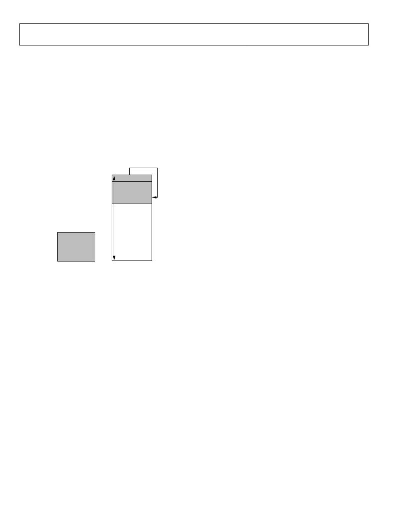
�A� useful� implementation� of� the� waterline� feature� is� to� determine�
�the� amount� of� space� required� for� the� stack� and� allow� a� suitable�
�default� starting� address� to� be� selected.� This� optimizes� the� use�
�of� the� additional� XRAM� space,� allowing� it� to� be� used� for� data�
�storage.� To� obtain� this� information,� the� waterline� should� be� set�
�to� the� estimated� stack� maximum� and� the� interrupt� enabled.�
�If� the� stack� exceeds� the� estimated� maximum,� the� interrupt� is� trig-�
�gered,� and� the� waterline� level� should� be� increased� in� the� interrupt�
�service� routine.� Before� returning� to� the� main� program,� the�
�waterline� interrupt� status� flag� (WTRLFG,� Bit� 0)� of� the� stack�
�boundary� SFR� (STCON,� Address� 0xBF)� should� be� cleared.� This�
�program� continues� to� jump� to� the� waterline� service� routine�
�until� the� stack� no� longer� exceeds� the� waterline� level� and� the�
�maximum� stack� level� is� determined.�
�0x7FF�
�Data� Sheet�
�Interrupt� SFR�
�A� two-tiered� interrupt� system� is� standard� in� the� 8052� core.� The�
�priority� level� for� each� interrupt� source� is� individually� select-able�
�as� high� or� low.� The� ADE5166/ADE5169/ADE5566/ADE5569�
�enhance� this� interrupt� system� by� creating,� in� essence,� a� third�
�interrupt� tier� for� a� highest� priority� power� supply� management�
�interrupt,� PSM� (see� the� Interrupt� System� section).�
�I/O� Port� SFRs�
�The� 8052� core� supports� four� I/O� ports,� P0� through� P3,� where�
�Port� 0� and� Port� 2� are� typically� used� for� access� to� external� code�
�and� data� spaces.� The� ADE5166/ADE5169/ADE5566/ADE5569,�
�unlike� standard� 8052� products,� provide� internal� nonvolatile�
�flash� memory� so� that� an� external� code� space� is� unnecessary.�
�The� on-chip� LCD� driver� requires� many� pins,� some� of� which� are�
�dedicated� for� LCD� functionality� and� others� that� can� be� configured�
�0x7FF-STCON[7:3]�
�{SPH[5:3],� 0x00}�
�WATERLINE�
�STACK� STARTING�
�ADDRESS�
�as� LCD� or� general-purpose� I/O.� Due� to� the� limited� number� of�
�I/O� pins,� the� ADE5166/ADE5169/ADE5566/ADE5569� do� not�
�allow� access� to� external� code� and� data� spaces.�
�The� ADE5166/ADE5169/ADE5566/ADE5569� provide� 20� pins�
�that� can� be� used� for� general-purpose� I/O.� These� pins� are� mapped�
�0xFF�
�0x00�
�2kB� OF�
�ON-CHIP� XRAM�
�256� BYTES�
�OF� RAM�
�(DATA)�
�0x00�
�Figure� 82.� Extended� Stack� Pointer� Operation�
�to� Port� 0,� Port� 1,� and� Port� 2� and� are� accessed� through� three� bit-�
�addressable� 8052� SFRs:� P0,� P1,� and� P2.� Another� enhanced�
�feature� of� the� ADE5166/ADE5169/ADE5566/ADE5569� is� that�
�the� weak� pull-ups� standard� on� 8052� Port� 1,� Port� 2,� and� Port� 3�
�can� be� disabled� to� make� open-drain� outputs,� as� is� standard� on�
�Port� 0.� The� weak� pull-ups� can� be� enabled� on� a� pin-by-pin� basis�
�(see� the� I/O� Ports� section).�
�STANDARD� 8052� SFRS�
�The� standard� 8052� SFRs� include� the� accumulator� (ACC),� B,� PSW,�
�DPTR,� and� SP� SFRs,� as� described� in� the� Basic� 8052� Registers�
�section.� The� 8052� also� defines� standard� timers,� serial� port� inter-�
�faces,� interrupts,� I/O� ports,� and� power-down� modes.�
�Timer� SFRs�
�The� 8052� contains� three� 16-bit� timers,� the� identical� Timer� 0� and�
�Timer� 1,� as� well� as� a� Timer� 2.� These� timers� can� also� function� as�
�event� counters.� Timer� 2� has� a� capture� feature� in� which� the� value�
�of� the� timer� can� be� captured� in� two� 8-bit� registers� upon� the�
�assertion� of� an� external� input� signal� (see� the� Timers� section).�
�Power� Control� Register� (PCON,� Address� 0x87)�
�The� 8052� core� defines� two� power-down� modes:� power-down�
�and� idle.� The� ADE5166/ADE5169/ADE5566/ADE5569�
�enhance� the� power� control� capability� of� the� traditional� 8052�
�MCU� with� additional� power� management� functions.� The�
�POWCON� SFR� (Address� 0xC5)� is� used� to� define� power� control�
�specific� functionality� for� the� ADE5166/ADE5169/ADE5566/�
�ADE5569.� The� program� control� SFR� (PCON,� Address� 0x87)� is�
�not� bit� addressable� (see� the� Power� Management� section).�
�The� ADE5166/ADE5169/ADE5566/ADE5569� provide� many�
�other� peripherals� not� standard� to� the� 8052� core,� for� example�
�Serial� Port� SFRs�
�The� two� full-duplex� serial� port� peripherals� each� require� two�
�registers:� one� for� setting� up� the� baud� rate� and� other� communication�
�parameters,� and� another� register� for� the� transmit/receive� buffer.�
�The� ADE5166/ADE5169/ADE5566/ADE5569� also� provide�
�enhanced� serial� port� functionality� with� a� dedicated� timer� for�
�baud� rate� generation� with� a� fractional� divisor� and� additional�
�error� detec-tion� (see� the� UART� Serial� Interface� section� and� the�
�UART2� Serial� Interface� section.)�
�?�
�?�
�?�
�?�
�?�
�?�
�?�
�?�
�?�
�?�
�ADE� energy� measurement� DSP�
�Full� RTC�
�LCD� driver�
�Battery� switchover/power� management�
�Temperature� ADC�
�Battery� ADC�
�SPI/I� 2� C� communication�
�Flash� memory� controller�
�Watchdog� timer�
�Secondary� UART� port�
�Rev.� D� |� Page� 84� of� 156�
�相关PDF资料 |
PDF描述 |
|---|---|
| VE-J1M-EX | CONVERTER MINIMOD DC/DC 10V 75W |
| VE-21M-EX | CONVERTER MOD DC/DC 10V 75W |
| VE-21R-EX | CONVERTER MOD DC/DC 7.5V 75W |
| AD9912A/PCBZ | BOARD EVALUATION FOR AD9912 |
| H1KXH-2636M | IDC CABLE - HPK26H/AE26M/X |
相关代理商/技术参数 |
参数描述 |
|---|---|
| EVAL-ADE5169F62EBZ | 制造商:Analog Devices 功能描述:EVALUATION BOARD FOR ADE5169 - Boxed Product (Development Kits) 制造商:Rochester Electronics LLC 功能描述: |
| EVAL-ADE5569F62EBZ | 制造商:AD 制造商全称:Analog Devices 功能描述:Single-Phase Energy Measurement IC with 8052 MCU, RTC, and LCD Driver |
| EVAL-ADE7169EBZ-2 | 功能描述:BOARD EVALUATION FOR ADE7169F16 RoHS:是 类别:编程器,开发系统 >> 评估演示板和套件 系列:- 标准包装:1 系列:PCI Express® (PCIe) 主要目的:接口,收发器,PCI Express 嵌入式:- 已用 IC / 零件:DS80PCI800 主要属性:- 次要属性:- 已供物品:板 |
| EVAL-ADE7169F16EB | 制造商:AD 制造商全称:Analog Devices 功能描述:Single-Phase Energy Measurement IC with 8052 MCU, RTC and LCD driver |
| EVAL-ADE7169F16EBZ | 制造商:Analog Devices 功能描述:Evaluation Board For ADE7169 制造商:Analog Devices 功能描述:EVAL BD FOR ADE7169 - Bulk |
发布紧急采购,3分钟左右您将得到回复。