- 您现在的位置:买卖IC网 > PDF目录223992 > HY27SA081G1M-VPEB (HYNIX SEMICONDUCTOR INC) 128M X 8 FLASH 1.8V PROM, 12000 ns, PDSO48 PDF资料下载
参数资料
| 型号: | HY27SA081G1M-VPEB |
| 厂商: | HYNIX SEMICONDUCTOR INC |
| 元件分类: | PROM |
| 英文描述: | 128M X 8 FLASH 1.8V PROM, 12000 ns, PDSO48 |
| 封装: | 12 X 17 MM, 0.70 MM HEIGHT, LEAD FREE, WSOP1-48 |
| 文件页数: | 11/45页 |
| 文件大小: | 675K |
| 代理商: | HY27SA081G1M-VPEB |
第1页第2页第3页第4页第5页第6页第7页第8页第9页第10页当前第11页第12页第13页第14页第15页第16页第17页第18页第19页第20页第21页第22页第23页第24页第25页第26页第27页第28页第29页第30页第31页第32页第33页第34页第35页第36页第37页第38页第39页第40页第41页第42页第43页第44页第45页
Rev 0.3 / May. 2004
19
Preliminary
HY27UA(08/16)1G1M Series
HY27SA(08/16)1G1M Series
1Gbit (128Mx8bit / 64Mx16bit) NAND Flash
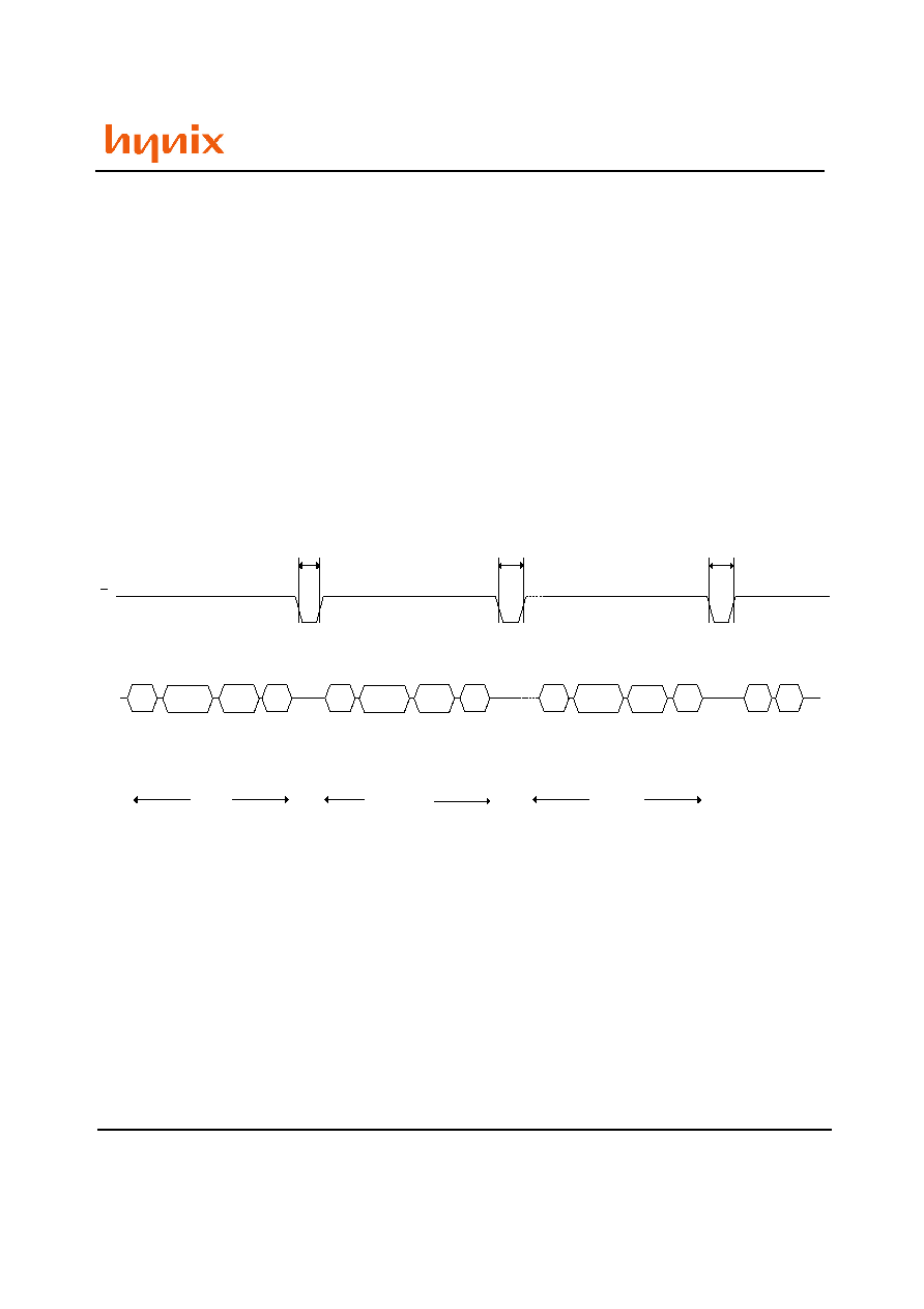
write cycles to input the address), the data is then input (up to 528 Bytes/ 264 Words) and loaded into the Cache Reg-
ister.
2. One bus cycle is required to issue the confirm command to start the P/E/R Controller.
3. The P/E/R Controller then transfers the data to the Page Buffer. During this the device is busy for a time of tBLBH5.
4. Once the data is loaded into the Page Buffer the P/E/R Controller programs the data into the memory array. As soon
as the Cache Registers are empty (after tBLBH5) a new Cache program command can be issued, while the internal pro-
gramming is still executing. Once the program operation has started the Status Register can be read using the Read
Status Register command. During Cache Program operations SR5 can be read to find out whether the internal pro-
gramming is ongoing (SR5 = '0') or has completed (SR5 = '1') while SR6 indicates whether the Cache Register is ready
to accept new data. If any errors have been detected on the previous page (Page N-1), the Cache Program Error Bit
SR1 will be set to '1', while if the error has been detected on Page N the Error Bit SR0 will be set to '1'. When the next
page ( Page N) of data is input with the Cache Program command, tBLBH5 is affected by the pending internal program-
ming. The data will only be transferred from the Cache Register to the Page Buffer when the pending program cycle is
finished and the Page Buffer is available. If the system monitors the progress of the operation using only the Ready/
Busy signal, the last page of data must be programmed with the Page Program confirm command (10h).
If the Cache Program confirm command (15h) is used instead, Status Register bit SR5 must be polled to find out if the
last programming is finished before starting any other operations.
Note: (1). tX is a fraction of the Program Busy Time and is less than tBLBH2.
(2). Up to 32 pages can be programmed in one Cache Program operation.
Block Erase
Erase operations are done one block at a time. An erase operation sets all of the bits in the addressed block to '1'. All
previous data in the block is lost. An erase operation consists of three steps (refer to Figure 17):
1. One bus cycle is required to setup the Block Erase command.
2. Only three bus cycles for the devices are required to input the block address. The first cycle (A0 to A7) is not
required as only addresses A14 to A26 (highest address depends on device density) are valid, A9 to A13 are ignored.
In the last address cycle I/O0 to I/O7 must be set to VIL.
3. One bus cycle is required to issue the confirm command to start the P/E/R Controller.
Figure 16. Cashe Program Operation
Page
Program
Code
Cache
Program
Code
Cache Program
Confirm Code
Page
Program
Code
Page
Program
Confirm Code
Read Status
Register
First Page
Last Page
Second Page
(can be repeated up to 30 times)
Busy
tBLBH5
(Cache Busy time)
tX(1)+tBLBH5
tX(1)+tBLBH5+tBLBH2
(Program Busy Time)
80h
15h
Data
Input
15h
Input
Address
80h
Input
Address
80h
Data
Input
10h
70h
Input
Address
SR0
Data
Input
RB
I/O
相关PDF资料 |
PDF描述 |
|---|---|
| HY27UA081G1M-TIB | 128M X 8 FLASH 3.3V PROM, 12000 ns, PDSO48 |
| HY27US08121B-TPIS | 64M X 8 FLASH 3.3V PROM, 18 ns, PDSO48 |
| HY27US08121B-FIB | 64M X 8 FLASH 3.3V PROM, 18 ns, PBGA63 |
| HY27US081G1MSES | 128M X 8 FLASH 2.7V PROM, 45 ns, PDSO48 |
| HY27US081G1MTCS | 128M X 8 FLASH 2.7V PROM, 45 ns, PDSO48 |
相关代理商/技术参数 |
参数描述 |
|---|---|
| HY27SA161G1M | 制造商:HYNIX 制造商全称:Hynix Semiconductor 功能描述:1Gbit (128Mx8bit / 64Mx16bit) NAND Flash Memory |
| HY27SA1G1M | 制造商:HYNIX 制造商全称:Hynix Semiconductor 功能描述:1Gbit (128Mx8bit / 64Mx16bit) NAND Flash Memory |
| HY27SAXXX | 制造商:HYNIX 制造商全称:Hynix Semiconductor 功能描述:1Gbit (128Mx8bit / 64Mx16bit) NAND Flash Memory |
| HY27SF081G2A | 制造商:HYNIX 制造商全称:Hynix Semiconductor 功能描述:1Gbit (128Mx8bit / 64Mx16bit) NAND Flash |
| HY27SF081G2A-F(P) | 制造商:SK Hynix Inc 功能描述: |
发布紧急采购,3分钟左右您将得到回复。