- 您现在的位置:买卖IC网 > PDF目录223992 > HY27SA081G1M-VPEB (HYNIX SEMICONDUCTOR INC) 128M X 8 FLASH 1.8V PROM, 12000 ns, PDSO48 PDF资料下载
参数资料
| 型号: | HY27SA081G1M-VPEB |
| 厂商: | HYNIX SEMICONDUCTOR INC |
| 元件分类: | PROM |
| 英文描述: | 128M X 8 FLASH 1.8V PROM, 12000 ns, PDSO48 |
| 封装: | 12 X 17 MM, 0.70 MM HEIGHT, LEAD FREE, WSOP1-48 |
| 文件页数: | 17/45页 |
| 文件大小: | 675K |
| 代理商: | HY27SA081G1M-VPEB |
第1页第2页第3页第4页第5页第6页第7页第8页第9页第10页第11页第12页第13页第14页第15页第16页当前第17页第18页第19页第20页第21页第22页第23页第24页第25页第26页第27页第28页第29页第30页第31页第32页第33页第34页第35页第36页第37页第38页第39页第40页第41页第42页第43页第44页第45页

Rev 0.3 / May. 2004
25
Preliminary
HY27UA(08/16)1G1M Series
HY27SA(08/16)1G1M Series
1Gbit (128Mx8bit / 64Mx16bit) NAND Flash
Bad Block Management
Devices with Bad Blocks have the same quality level and the same AC and DC characteristics as devices where all the
blocks are valid. A Bad Block does not affect the performance of valid blocks because it is isolated from the bit line and
common source line by a select transistor.
The devices are supplied with all the locations inside valid blocks erased (FFh). The Bad Block Information is written
prior to shipping. Any block where the 6th Byte/ 1st Word in the spare area of the 1st or 2nd page (if the 1st page is
Bad) does not contain FFh is a Bad Block.
The Bad Block Information must be read before any erase is attempted as the Bad Block Information may be erased.
For the system to be able to recognize the Bad Blocks based on the original information it is recommended to create a
Bad Block table following the flowchart shown in Figure 20.
Block Replacement
Over the lifetime of the device additional Bad Blocks may develop. In this case the block has to be replaced by copying
the data to a valid block.
These additional Bad Blocks can be identified as attempts to program or erase them will give errors in the Status Reg-
ister.
As the failure of a page program operation does not affect the data in other pages in the same block, the block can be
replaced by re-programming the current data and copying the rest of the replaced block to an available valid block.
The Copy Back Program command can be used to copy the data to a valid block.
See the “Copy Back Program” section for more details.
Refer to Table 7 for the recommended procedure to follow if an error occurs during an operation.
Table 7: Block Failure
Operation
Recommended Procedure
Erase
Block Replacement
Program
Block Replacement or ECC
Read
ECC
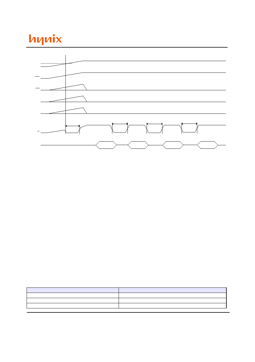
Note: (1). VCCth is equal to 2.5V for 3V Power Supply devices.
Figure 19. Automatic Page 0 Read at power-up (Sequential Row Read Enable)
Vccth(1)
Vcc
WE
CE
ALE
CLE
RB
I/O
tBLBH1
(Read Busy time)
Busy
tBLBH1
Page 0
Data Out
Page 1
Data Out
Page 2
Data Out
Page Nth
Data Out
相关PDF资料 |
PDF描述 |
|---|---|
| HY27UA081G1M-TIB | 128M X 8 FLASH 3.3V PROM, 12000 ns, PDSO48 |
| HY27US08121B-TPIS | 64M X 8 FLASH 3.3V PROM, 18 ns, PDSO48 |
| HY27US08121B-FIB | 64M X 8 FLASH 3.3V PROM, 18 ns, PBGA63 |
| HY27US081G1MSES | 128M X 8 FLASH 2.7V PROM, 45 ns, PDSO48 |
| HY27US081G1MTCS | 128M X 8 FLASH 2.7V PROM, 45 ns, PDSO48 |
相关代理商/技术参数 |
参数描述 |
|---|---|
| HY27SA161G1M | 制造商:HYNIX 制造商全称:Hynix Semiconductor 功能描述:1Gbit (128Mx8bit / 64Mx16bit) NAND Flash Memory |
| HY27SA1G1M | 制造商:HYNIX 制造商全称:Hynix Semiconductor 功能描述:1Gbit (128Mx8bit / 64Mx16bit) NAND Flash Memory |
| HY27SAXXX | 制造商:HYNIX 制造商全称:Hynix Semiconductor 功能描述:1Gbit (128Mx8bit / 64Mx16bit) NAND Flash Memory |
| HY27SF081G2A | 制造商:HYNIX 制造商全称:Hynix Semiconductor 功能描述:1Gbit (128Mx8bit / 64Mx16bit) NAND Flash |
| HY27SF081G2A-F(P) | 制造商:SK Hynix Inc 功能描述: |
发布紧急采购,3分钟左右您将得到回复。