- 您现在的位置:买卖IC网 > PDF目录223992 > HY27SA081G1M-VPEB (HYNIX SEMICONDUCTOR INC) 128M X 8 FLASH 1.8V PROM, 12000 ns, PDSO48 PDF资料下载
参数资料
| 型号: | HY27SA081G1M-VPEB |
| 厂商: | HYNIX SEMICONDUCTOR INC |
| 元件分类: | PROM |
| 英文描述: | 128M X 8 FLASH 1.8V PROM, 12000 ns, PDSO48 |
| 封装: | 12 X 17 MM, 0.70 MM HEIGHT, LEAD FREE, WSOP1-48 |
| 文件页数: | 15/45页 |
| 文件大小: | 675K |
| 代理商: | HY27SA081G1M-VPEB |
第1页第2页第3页第4页第5页第6页第7页第8页第9页第10页第11页第12页第13页第14页当前第15页第16页第17页第18页第19页第20页第21页第22页第23页第24页第25页第26页第27页第28页第29页第30页第31页第32页第33页第34页第35页第36页第37页第38页第39页第40页第41页第42页第43页第44页第45页
Rev 0.3 / May. 2004
22
Preliminary
HY27UA(08/16)1G1M Series
HY27SA(08/16)1G1M Series
1Gbit (128Mx8bit / 64Mx16bit) NAND Flash
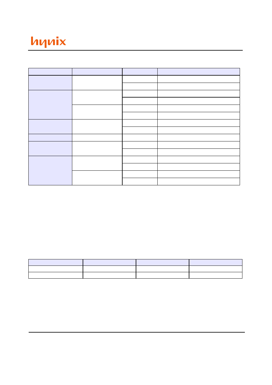
Table 6: Status Register Bit
Note: (1). The SR6 bit and SR0 bit have a different meaning during Cache Program operations.
(2). Only valid for Cache Program operations, for other operations it is same as SR6.
(3). Only valid for Cache Program operations, for other operations it is Don't Care.
Read Electronic Signature
The device contains a Manufacturer Code and Device Code. To read these codes two steps are required:
1. first use one Bus Write cycle to issue the Read Electronic Signature command (90h)
2. then subsequent Bus Read operations will read the Manufacturer Code and the Device Code until another command
is issued.
Refer to Table, Read Electronic Signature for information on the addresses.
Automatic Page 0 Read at Power-Up
Automatic Page 0 Read at Power-Up is an option available on all devices belonging to the NAND Flash 528 Byte/264
Word Page family. It allows the microcontroller to directly download boot code from page 0, without requiring any
command or address input sequence. The Automatic Page 0 Read option is particularly suited for applications that
boot from the NAND.
Devices delivered with Automatic Page 0 Read at Power-Up can have the Sequential Row Read option either enabled
or disabled.
Bit
NAME
Logic Level
Definition
SR7
Write Protection
'1'
Not Protected
'0'
Protected
SR6(1)
Program/Erase/Read
Controller
'1'
P/E/R C Inactive, device ready
'0'
P/E/R C active, device busy
Cache Read/Busy
'1'
Cache Register ready (Cache Program only)
'0'
Cache Register busy (Cache Program only)
SR5
Program/ Erase/ Read
Controller(2)
'1'
P/E/R C inactive, device ready
'0'
P/E/R C active, device busy
SR4, SR3, SR2
Reserved
Don
't Care
SR1
Cache Program Error(3)
'1'
Page N-1 failed in Cache Program operation
'0'
Page N-1 programmed successfully
SR0(1)
Generic Error
'1'
Error - Operation failed
'0'
No Error - Operation successful
Cache Program Error
'1'
Page N failed in Cache Program operation
'0'
Page N programmed successfully
Part Number
Manufacture Code
Device Code
Bus Width
HY27(U/S)A081G1M
ADh
79h
x8
HY27(U/S)A161G1M
00ADh
0074h
x16
相关PDF资料 |
PDF描述 |
|---|---|
| HY27UA081G1M-TIB | 128M X 8 FLASH 3.3V PROM, 12000 ns, PDSO48 |
| HY27US08121B-TPIS | 64M X 8 FLASH 3.3V PROM, 18 ns, PDSO48 |
| HY27US08121B-FIB | 64M X 8 FLASH 3.3V PROM, 18 ns, PBGA63 |
| HY27US081G1MSES | 128M X 8 FLASH 2.7V PROM, 45 ns, PDSO48 |
| HY27US081G1MTCS | 128M X 8 FLASH 2.7V PROM, 45 ns, PDSO48 |
相关代理商/技术参数 |
参数描述 |
|---|---|
| HY27SA161G1M | 制造商:HYNIX 制造商全称:Hynix Semiconductor 功能描述:1Gbit (128Mx8bit / 64Mx16bit) NAND Flash Memory |
| HY27SA1G1M | 制造商:HYNIX 制造商全称:Hynix Semiconductor 功能描述:1Gbit (128Mx8bit / 64Mx16bit) NAND Flash Memory |
| HY27SAXXX | 制造商:HYNIX 制造商全称:Hynix Semiconductor 功能描述:1Gbit (128Mx8bit / 64Mx16bit) NAND Flash Memory |
| HY27SF081G2A | 制造商:HYNIX 制造商全称:Hynix Semiconductor 功能描述:1Gbit (128Mx8bit / 64Mx16bit) NAND Flash |
| HY27SF081G2A-F(P) | 制造商:SK Hynix Inc 功能描述: |
发布紧急采购,3分钟左右您将得到回复。