- 您现在的位置:买卖IC网 > PDF目录67712 > IDT72T6360L6BBGI (INTEGRATED DEVICE TECHNOLOGY INC) SPECIALTY MICROPROCESSOR CIRCUIT, PBGA324 PDF资料下载
参数资料
| 型号: | IDT72T6360L6BBGI |
| 厂商: | INTEGRATED DEVICE TECHNOLOGY INC |
| 元件分类: | 微控制器/微处理器 |
| 英文描述: | SPECIALTY MICROPROCESSOR CIRCUIT, PBGA324 |
| 封装: | 19 X 19 MM, 1 MM PITCH, PLASTIC, BGA-324 |
| 文件页数: | 50/51页 |
| 文件大小: | 508K |
| 代理商: | IDT72T6360L6BBGI |
第1页第2页第3页第4页第5页第6页第7页第8页第9页第10页第11页第12页第13页第14页第15页第16页第17页第18页第19页第20页第21页第22页第23页第24页第25页第26页第27页第28页第29页第30页第31页第32页第33页第34页第35页第36页第37页第38页第39页第40页第41页第42页第43页第44页第45页第46页第47页第48页第49页当前第50页第51页
8
IDT72T6360 2.5V, SEQUENTIAL FLOW-CONTROL DEVICE
x9, x18, x36 BIT WIDE CONFIGURATION
COMMERCIALANDINDUSTRIAL
TEMPERATURERANGES
OCTOBER 10, 2005
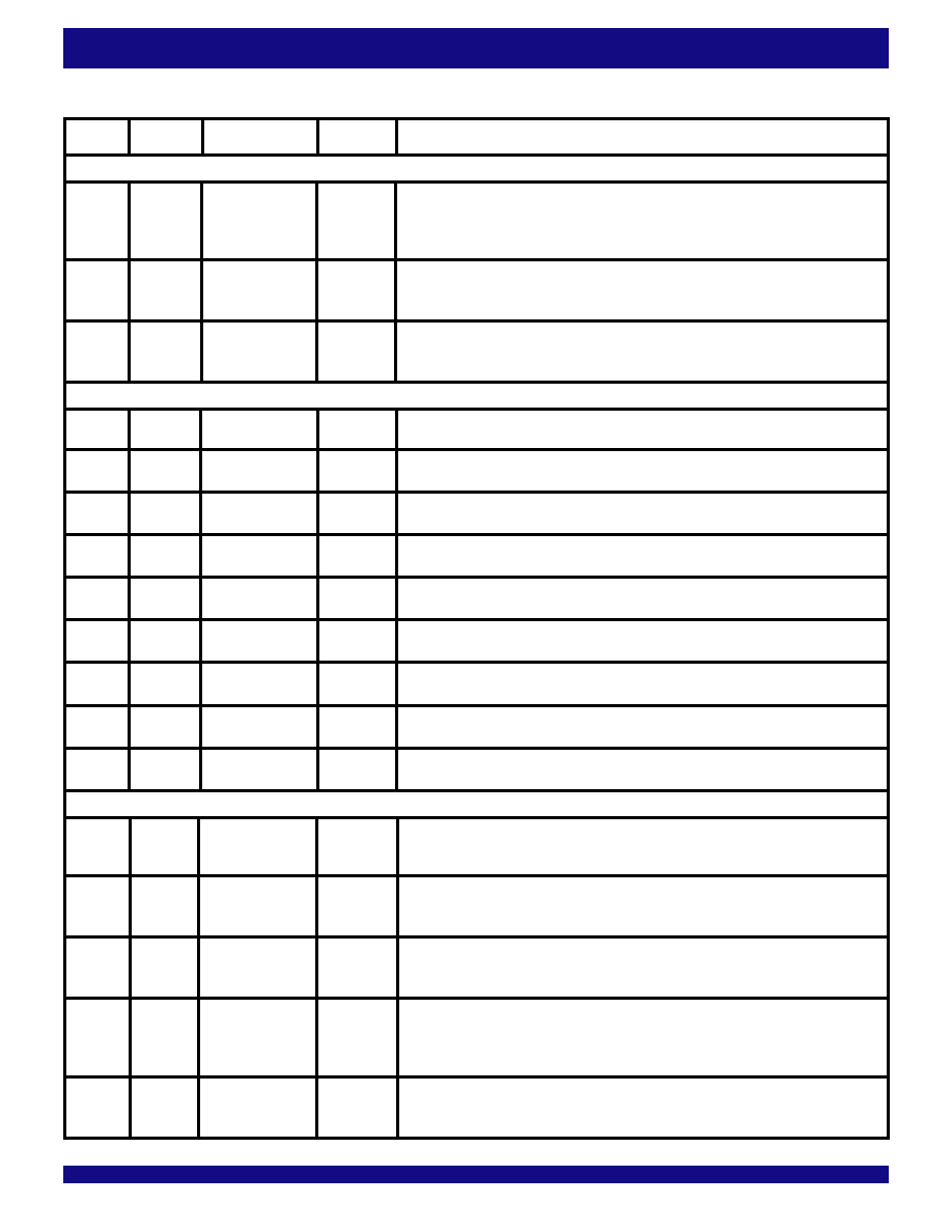
WRITE PORT INTERFACE (Continued)
WCLK/WR
V8
WriteClock/
INPUT
This is a dual function pin. If synchronous operation of the write port is selected, the rising
WriteStrobe
3.3V or
edge of WCLK writes data into the sequential flow-control device when
WEN is enabled.
2.5V LVTTL If asynchronous operation of the write port is selected, a rising edge on WR writes data into
the sequential flow-control device without the need of a free-running input write clock.
WCS
T7
WriteChipSelect
INPUT
Synchronous three-state control of the data inputs. Provides a means of controlling the
3.3V or
data inputs synchronous to WCLK. Typically used to avoid bus-contention when multiple
2.5V LVTTL devices are sharing the same input data bus.
WEN
V7
WriteEnable
INPUT
WEN enables WCLK for writing data into the sequential flow-control device. If
3.3V or
asynchronous mode is selected on the write port, this signal should be tied to GND.
2.5V LVTTL
MEMORY INTERFACE
A[12:0]
See Pin
Memory Address
OUTPUT
Output address bus to be connected to the input address bus of the external memory to
No. table
Bus
SSTL_2
provide row and column address.
BA[1:0]
BA1-B11
Memory Bank
OUTPUT
Address bits to be connected to the external memory's BA inputs to determine which bank
BA0-C11
Address Input Bit
SSTL_2
an ACTIVE, READ, WRITE, or PRECHARGE command is being applied.
CK
C7
Memory Clock
OUTPUT
Clock output to be connected to the external memory's input clock.
SSTL_2
CK
A7
Memory Clock
OUTPUT
Differential clock output to be connected to the external memory's differential input clock.
Inverted
SSTL_2
CAS
D12
Memory Column
OUTPUT
Output enable signal to be connected to the external memory's
CAS pin to activate and
Address Strobe
SSTL_2
deactivate the column address strobe.
DQ[63:0]
See Pin
Memory Data Bus
Bi-Directional Input/output data bus for the external memory's data bus.
No. table
SSTL_2
DQS[7:0]
See Pin
Memory Data
Bi-Directional Input/output data strobe to be connected to the external memory's data strobe.
No. table
Strobe
SSTL_2
RAS
A12
Memory Row
OUTPUT
Output strobe signal to be connected to the external memory's
RAS pin to activate and
Address Strobe
SSTL_2
deactivate the row address strobe.
WE
A11
MemoryWrite
OUTPUT
Output strobe signal to be connected to the external memory's
WE pin to activate and
Enable
SSTL_2
deactivate the write address strobe.
CONTROL AND FEATURE INTERFACE
BM[3:0](1)
See Pin
Bus-MatchingBit
INPUT
Selects the bus width of the read and write ports.
No. table
3.3V or
2.5V LVTTL
FSEL[1:0](1)
FSEL1-P6 Flag Select Bit
INPUT
During master reset, these inputs will select one of four default values for the programmable
FSEL0-R6
3.3V or
flags
PAE and PAF. The selected value will apply to both PAE and PAF offset.
2.5V LVTTL
FWFT(1)
U7
First Word Fall
INPUT
During master reset, a HIGH on this input selects FWFT timing mode. A LOW selects IDT
Through
3.3V or
Standardtimingmode.
2.5V LVTTL
IDEM(1)
R7
IDT Standard Mode
INPUT
This select pin is used for depth expansion configuration in IDT Standard mode. If this pin
Depth Expansion
3.3V or
is tied HIGH, then the
FF/IR signal will be inverted to provide a seamless depth
Mode Select
2.5V LVTTL expansion interface. If depth expansion in FWFT mode is desired, this pin should be
tied to GND. If no depth expansion is used, this pin should be tied to GND.
IOSEL(1)
P7
I/O VDDQ Select
INPUT
This input determines whether the inputs and outputs will tolerate a 2.5V or 3.3V voltage
3.3V or
signals. If IOSEL is HIGH, then all I/Os will be 2.5V tolerant. If IOSEL is LOW, then all I/Os
2.5V LVTTL will be 3.3V tolerant. See table 15, for a list of affected I/O signals.
PIN DESCRIPTIONS (Continued)
Symbol
Pin No.
Name
I/O TYPE
Description
Location
相关PDF资料 |
PDF描述 |
|---|---|
| IDT73210ATC | 73 SERIES, 9-BIT REGISTERED TRANSCEIVER, TRUE OUTPUT, CDIP24 |
| IDT73211ATCB | 73 SERIES, 9-BIT REGISTERED TRANSCEIVER, TRUE OUTPUT, CDIP24 |
| IDT73210TC | 73 SERIES, 9-BIT REGISTERED TRANSCEIVER, TRUE OUTPUT, CDIP24 |
| IDT73211TCB | 73 SERIES, 9-BIT REGISTERED TRANSCEIVER, TRUE OUTPUT, CDIP24 |
| IDT73210ATCB | 73 SERIES, 9-BIT REGISTERED TRANSCEIVER, TRUE OUTPUT, CDIP24 |
相关代理商/技术参数 |
参数描述 |
|---|---|
| IDT72T6360L7-5BB | 功能描述:IC FLOW-CTRL 48BIT 7-5NS 324-BGA RoHS:否 类别:集成电路 (IC) >> 专用 IC 系列:- 产品培训模块:Lead (SnPb) Finish for COTS Obsolescence Mitigation Program 标准包装:1 系列:- 类型:调帧器 应用:数据传输 安装类型:表面贴装 封装/外壳:400-BBGA 供应商设备封装:400-PBGA(27x27) 包装:散装 |
| IDT72T6360L7-5BBI | 功能描述:IC FLOW-CTRL 48BIT 7-5NS 324-BGA RoHS:否 类别:集成电路 (IC) >> 专用 IC 系列:- 产品培训模块:Lead (SnPb) Finish for COTS Obsolescence Mitigation Program 标准包装:1 系列:- 类型:调帧器 应用:数据传输 安装类型:表面贴装 封装/外壳:400-BBGA 供应商设备封装:400-PBGA(27x27) 包装:散装 |
| IDT72T6480L10BB | 功能描述:IC FLOW-CTRL 48BIT 10NS 324-BGA RoHS:否 类别:集成电路 (IC) >> 专用 IC 系列:- 产品培训模块:Lead (SnPb) Finish for COTS Obsolescence Mitigation Program 标准包装:1 系列:- 类型:调帧器 应用:数据传输 安装类型:表面贴装 封装/外壳:400-BBGA 供应商设备封装:400-PBGA(27x27) 包装:散装 |
| IDT72T6480L10BBI | 功能描述:IC FLOW-CTRL 48BIT 10NS 324-BGA RoHS:否 类别:集成电路 (IC) >> 专用 IC 系列:- 产品培训模块:Lead (SnPb) Finish for COTS Obsolescence Mitigation Program 标准包装:1 系列:- 类型:调帧器 应用:数据传输 安装类型:表面贴装 封装/外壳:400-BBGA 供应商设备封装:400-PBGA(27x27) 包装:散装 |
| IDT72T6480L7-5BB | 功能描述:IC FLOW-CTRL 48BIT 7-5NS 324-BGA RoHS:否 类别:集成电路 (IC) >> 专用 IC 系列:- 产品培训模块:Lead (SnPb) Finish for COTS Obsolescence Mitigation Program 标准包装:1 系列:- 类型:调帧器 应用:数据传输 安装类型:表面贴装 封装/外壳:400-BBGA 供应商设备封装:400-PBGA(27x27) 包装:散装 |
发布紧急采购,3分钟左右您将得到回复。