- 您现在的位置:买卖IC网 > PDF目录80499 > M38D59GC-XXXFP 8-BIT, MROM, 6.25 MHz, MICROCONTROLLER, PQFP80 PDF资料下载
参数资料
| 型号: | M38D59GC-XXXFP |
| 元件分类: | 微控制器/微处理器 |
| 英文描述: | 8-BIT, MROM, 6.25 MHz, MICROCONTROLLER, PQFP80 |
| 封装: | 14 X 20 MM, 0.80 MM PITCH, PLASTIC, QFP-80 |
| 文件页数: | 117/142页 |
| 文件大小: | 2004K |
| 代理商: | M38D59GC-XXXFP |
第1页第2页第3页第4页第5页第6页第7页第8页第9页第10页第11页第12页第13页第14页第15页第16页第17页第18页第19页第20页第21页第22页第23页第24页第25页第26页第27页第28页第29页第30页第31页第32页第33页第34页第35页第36页第37页第38页第39页第40页第41页第42页第43页第44页第45页第46页第47页第48页第49页第50页第51页第52页第53页第54页第55页第56页第57页第58页第59页第60页第61页第62页第63页第64页第65页第66页第67页第68页第69页第70页第71页第72页第73页第74页第75页第76页第77页第78页第79页第80页第81页第82页第83页第84页第85页第86页第87页第88页第89页第90页第91页第92页第93页第94页第95页第96页第97页第98页第99页第100页第101页第102页第103页第104页第105页第106页第107页第108页第109页第110页第111页第112页第113页第114页第115页第116页当前第117页第118页第119页第120页第121页第122页第123页第124页第125页第126页第127页第128页第129页第130页第131页第132页第133页第134页第135页第136页第137页第138页第139页第140页第141页第142页
Rev.3.04
May 20, 2008
REJ03B0158-0304
38D5 Group
Outline Performance
CPU rewrite mode is usable in the single-chip or Boot mode. The
only User ROM area can be rewritten.
In CPU rewrite mode, the CPU erases, programs and reads the
internal flash memory as instructed by software commands. This
rewrite control program must be transferred to internal RAM
area before it can be executed.
The MCU enters CPU rewrite mode by setting “1” to the CPU
rewrite mode select bit (bit 1 of address 0FE016). Then, software
commands can be accepted.
Use software commands to control program and erase
operations. Whether a program or erase operation has terminated
normally or in error can be verified by reading the status register.
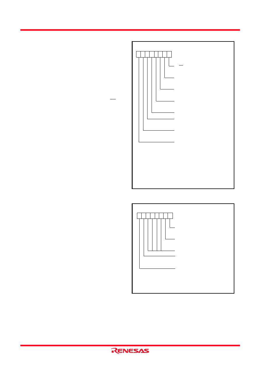
Figure 71 shows the flash memory control register 0.
Bit 0 of the flash memory control register 0 is the RY/BY status
flag used exclusively to read the operating status of the flash
memory. During programming and erase operations, it is “0”
(busy). Otherwise, it is “1” (ready).
Bit 1 of the flash memory control register 0 is the CPU rewrite
mode select bit. When this bit is set to “1”, the MCU enters CPU
rewrite mode. And then, software commands can be accepted. In
CPU rewrite mode, the CPU becomes unable to access the
internal flash memory directly. Therefore, use the control
program in the internal RAM for write to bit 1. To set this bit 1 to
“1”, it is necessary to write “0” and then write “1” in succession
to bit 1. The bit can be set to “0” by only writing “0”.
Bit 2 of the flash memory control register 0 is the user block 1
E/W enable bit. By setting combination of bit 4 (user block 0
E/W enable bit) of the flash memory control register 2 (address
user block in the CPU rewriting mode.
Bit 3 of the flash memory control register 0 is the flash memory
reset bit used to reset the control circuit of internal flash memory.
This bit is used when flash memory access has failed. When the
CPU rewrite mode select bit is “1”, setting “1” for this bit resets
the control circuit. To release the reset, it is necessary to set this
bit to “0”.
Bit 5 of the flash memory control register 0 is the User ROM
area select bit and is valid only in the boot mode. Setting this bit
to “1” in the boot mode switches an accessible area from the boot
ROM area to the user ROM area. To use the CPU rewrite mode
in the boot mode, set this bit to “1”. To rewrite bit 5, execute the
user original reprogramming control software transferred to the
internal RAM in advance.
Bit 6 of the flash memory control register 0 is the program status
flag. This bit is set to “1” when writing to flash memory is failed.
When program error occurs, the block cannot be used.
Bit 7 of the flash memory control register 0 is the erase status
flag.
This bit is set to “1” when erasing flash memory is failed. When
erase error occurs, the block cannot be used.
Figure 72 shows the flash memory control register 1.
Bit 0 of the flash memory control register 1 is the Erase suspend
enable bit. By setting this bit to “1”, the erase suspend mode to
suspend erase processing temporary when block erase command
is executed can be used. In order to set this bit 0 to “1”, writing
“0” and “1” in succession to bit 0. In order to set this bit to “0”,
write “0” only to bit 0.
Bit 1 of the flash memory control register 1 is the erase suspend
request bit. By setting this bit to “1” when erase suspend enable
bit is “1”, the erase processing is suspended.
Bit 6 of the flash memory control register 1 is the erase suspend
flag. This bit is cleared to “0” at the flash erasing.
Fig 71. Structure of flash memory control register 0
Fig 72. Structure of flash memory control register 1
Flash memory control register 0
(FMCR0: address : 0FE016, initial value: 0116)
RY/BY status flag
0 : Busy (being written or erased)
1 : Ready
CPU rewrite mode select bit(1)
0 : CPU rewrite mode invalid
1 : CPU rewrite mode valid
User block 1 E/W enable bit(1, 2)
0 : E/W disabled (180016-7FFF16)
1 : E/W enabled (180016-7FFF16)
Flash memory reset bit(3, 4)
0 : Normal operation
1 : reset
Not used (do not write “1” to this bit.)
User ROM area select bit(5)
0 : Boot ROM area is accessed
1 : User ROM area is accessed
Program status flag
0: Pass
1: Error
Erase status flag
0: Pass
1: Error
b7
b0
Notes 1: For this bit to be set to “1”, the user needs to write a “0” and then a
“1” to it in succession. For this bit to be set to “0”, write “0” only to
this bit.
2: This bit can be written only when CPU rewrite mode select bit is “1”.
3: Effective only when the CPU rewrite mode select bit = “1”. Fix this
bit to “0” when the CPU rewrite mode select bit is “0”.
4: When setting this bit to “1” (when the control circuit of flash memory
is reset), the flash memory cannot be accessed for 10 ms.
5: Write to this bit in program on RAM
Flash memory control register 1
(FMCR1: address: 0FE116, initial value: 4016)
Erase Suspend enable bit(1)
0 : Suspend invalid
1 : Suspend valid
Erase Suspend request bit(2)
0 : Erase restart
1 : Suspend request
Not used (do not write “1” to this bit.)
Erase Suspend flag
0 : Erase active
1 : Erase inactive (Erase Suspend mode)
Not used (do not write “1” to this bit.)
b7
b0
Notes 1: For this bit to be set to “1”, the user needs to write a “0” and then a
“1” to it in succession. For this bit to be set to “0”, write “0” only to
this bit.
2: Effective only when the suspend enable bit = “1”.
相关PDF资料 |
PDF描述 |
|---|---|
| MC68B05P2L | 8-BIT, MROM, 2 MHz, MICROCONTROLLER, CDIP28 |
| MC908QB4MDT | 8-BIT, FLASH, 8 MHz, MICROCONTROLLER, PDSO16 |
| MC908QY2AVDWE | 8-BIT, FLASH, 8 MHz, MICROCONTROLLER, PDSO16 |
| MK2745-20SLF | 108 MHz, VIDEO CLOCK GENERATOR, PDSO16 |
| MK2742-04SLFTR | 81 MHz, VIDEO CLOCK GENERATOR, PDSO16 |
相关代理商/技术参数 |
参数描述 |
|---|---|
| M38D59GFFP#U0 | 功能描述:IC 740/38D5 MCU QZ-ROM 80QFP RoHS:是 类别:集成电路 (IC) >> 嵌入式 - 微控制器, 系列:740/38000 标准包装:250 系列:80C 核心处理器:8051 芯体尺寸:8-位 速度:16MHz 连通性:EBI/EMI,I²C,UART/USART 外围设备:POR,PWM,WDT 输入/输出数:40 程序存储器容量:- 程序存储器类型:ROMless EEPROM 大小:- RAM 容量:256 x 8 电压 - 电源 (Vcc/Vdd):4.5 V ~ 5.5 V 数据转换器:A/D 8x10b 振荡器型:内部 工作温度:-40°C ~ 85°C 封装/外壳:68-LCC(J 形引线) 包装:带卷 (TR) |
| M38D59GFHP#U0 | 功能描述:IC 740/38D5 MCU QZ-ROM 80LQFP RoHS:是 类别:集成电路 (IC) >> 嵌入式 - 微控制器, 系列:740/38000 标准包装:250 系列:80C 核心处理器:8051 芯体尺寸:8-位 速度:16MHz 连通性:EBI/EMI,I²C,UART/USART 外围设备:POR,PWM,WDT 输入/输出数:40 程序存储器容量:- 程序存储器类型:ROMless EEPROM 大小:- RAM 容量:256 x 8 电压 - 电源 (Vcc/Vdd):4.5 V ~ 5.5 V 数据转换器:A/D 8x10b 振荡器型:内部 工作温度:-40°C ~ 85°C 封装/外壳:68-LCC(J 形引线) 包装:带卷 (TR) |
| M38D59T-RLFS | 功能描述:BOARD EMULATOR FOR 38D5 GROUP RoHS:否 类别:编程器,开发系统 >> 内电路编程器、仿真器以及调试器 系列:- 产品变化通告:Development Systems Discontinuation 19/Jul/2010 标准包装:1 系列:* 类型:* 适用于相关产品:* 所含物品:* |
| M38DC-15 | 制造商:M/A-COM Technology Solutions 功能描述:MIXER(SPEC UX1015) - Bulk |
| M38K00F1-16FP | 制造商:MITSUBISHI 制造商全称:Mitsubishi Electric Semiconductor 功能描述:SINGLE-CHIP 8-BIT CMOS MICROCOMPUTER |
发布紧急采购,3分钟左右您将得到回复。