- 您现在的位置:买卖IC网 > PDF目录80499 > M38D59GC-XXXFP 8-BIT, MROM, 6.25 MHz, MICROCONTROLLER, PQFP80 PDF资料下载
参数资料
| 型号: | M38D59GC-XXXFP |
| 元件分类: | 微控制器/微处理器 |
| 英文描述: | 8-BIT, MROM, 6.25 MHz, MICROCONTROLLER, PQFP80 |
| 封装: | 14 X 20 MM, 0.80 MM PITCH, PLASTIC, QFP-80 |
| 文件页数: | 89/142页 |
| 文件大小: | 2004K |
| 代理商: | M38D59GC-XXXFP |
第1页第2页第3页第4页第5页第6页第7页第8页第9页第10页第11页第12页第13页第14页第15页第16页第17页第18页第19页第20页第21页第22页第23页第24页第25页第26页第27页第28页第29页第30页第31页第32页第33页第34页第35页第36页第37页第38页第39页第40页第41页第42页第43页第44页第45页第46页第47页第48页第49页第50页第51页第52页第53页第54页第55页第56页第57页第58页第59页第60页第61页第62页第63页第64页第65页第66页第67页第68页第69页第70页第71页第72页第73页第74页第75页第76页第77页第78页第79页第80页第81页第82页第83页第84页第85页第86页第87页第88页当前第89页第90页第91页第92页第93页第94页第95页第96页第97页第98页第99页第100页第101页第102页第103页第104页第105页第106页第107页第108页第109页第110页第111页第112页第113页第114页第115页第116页第117页第118页第119页第120页第121页第122页第123页第124页第125页第126页第127页第128页第129页第130页第131页第132页第133页第134页第135页第136页第137页第138页第139页第140页第141页第142页
Rev.3.04
May 20, 2008
REJ03B0158-0304
38D5 Group
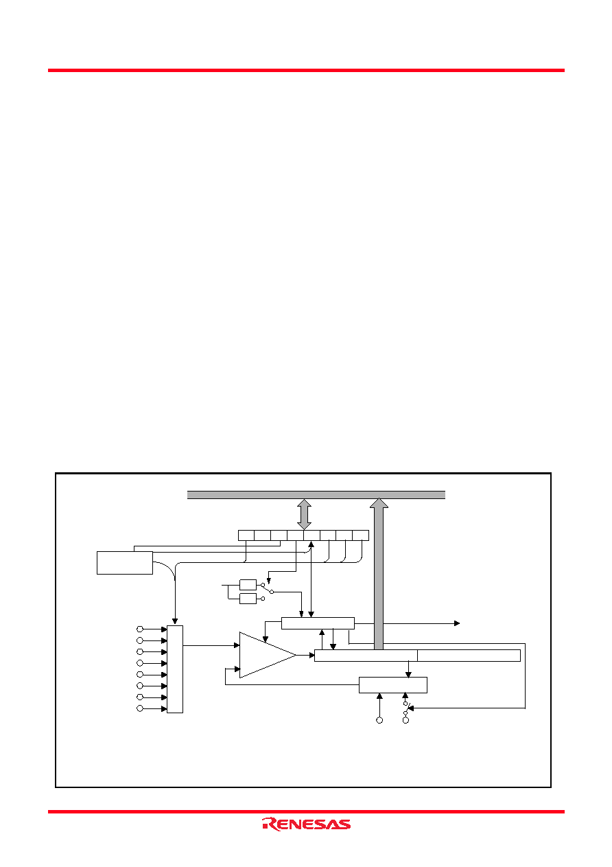
A/D CONVERTER
The 38D5 Group has a 10-bit A/D converter. The A/D converter
performs successive approximation conversion. The 38D5 Group
has the ADKEY function which perform A/D conversion of the
“L” level analog input from the ADKEY pin automatically.
[AD Conversion Register (ADL, ADH)]
One of these registers is a high-order register, and the other is a
low-order register. The high-order 8 bits of a conversion result is
stored in the AD conversion register (high-order) (address
001716), and the low-order 2 bits of the same result are stored in
bit 7 and bit 6 of the AD conversion register (low-order) (address
001616).
During A/D conversion, do not read these registers.
Also, the connection between the resistor ladder and reference
voltage input pin (VREF) can be controlled by the VREF input
switch bit (bit 0 of address 001616). When “1” is written to this
bit, the resistor ladder is always connected to VREF. When “0” is
written to this bit, the resistor ladder is disconnected from VREF
except during the A/D conversion.
[AD Control Register (ADCON)]
This register controls A/D converter. Bits 2 to 0 are analog input
pin selection bits. Bit 3 is an AD conversion completion bit and
“0” during A/D conversion. This bit is set to “1” upon
completion of A/D conversion.
A/D conversion is started by setting “0” in this bit.
Bit 5 is the ADKEY enable bit. The ADKEY function is enabled
by setting “1” to this bit. When this function is valid, the analog
input pin selection bits are ignored. Also, when bit 5 is “1”, do
not set “0” to bit 3 by program.
[Comparison Voltage Generator]
The comparison voltage generator divides the voltage between
AVSS and VREF, and outputs the divided voltages.
[Channel Selector]
The channel selector selects one of the input ports P57/AN7
P50/AN0 and inputs it to the comparator.
[Comparator and Control Circuit]
The comparator and control circuit compare an analog input
voltage with the comparison voltage and store the result in the
AD conversion register. When an A/D conversion is completed,
the control circuit sets the AD conversion completion bit and the
AD conversion interrupt request bit to “1”.
The comparator is constructed linked to a capacitor. The
conversion accuracy may be low because the change is lost if the
conversion speed is not enough.
Accordingly, set f(XIN) to at least 500 kHz during A/D
conversion in the XIN mode.
Also, do not execute the STP and WIT instructions during the
A/D conversion.
In the low-speed mode and on-chip oscillator mode, there is no
limit on the oscillation frequency because the on-chip oscillator
is used as the A/D conversion clock. In the low-speed mode, on-
chip oscillator starts oscillation automatically at the A/D
conversion is executed and stops oscillation automatically at the
A/D conversion is finished even though it is not oscillating.
Fig. 41 Block diagram of A/D converter
(Address 001716)
(Address 001616)
ADKEY
control circuit
AVSS
b7
b0
AD conversion register (L)
Data bus
C
h
a
n
e
lse
le
cto
r
AD conversion register (H)
Resistor ladder
Comparator
A/D interrupt request
AD control register
P50/AN0
P51/AN1
P52/AN2
P53/AN3
P54/AN4
P55/AN5
P56/AN6
P57/AN7/ADKEY0
VREF
1/ 8
1/ 2
φSOURCE
Note 1:
φSOURCE indicates the followings:
XIN input in the frequency/2, 4, or 8 mode
On-chip oscillator divided by 4 in the low-speed and the on-chip oscillator mode
A/D control circuit
(1)
相关PDF资料 |
PDF描述 |
|---|---|
| MC68B05P2L | 8-BIT, MROM, 2 MHz, MICROCONTROLLER, CDIP28 |
| MC908QB4MDT | 8-BIT, FLASH, 8 MHz, MICROCONTROLLER, PDSO16 |
| MC908QY2AVDWE | 8-BIT, FLASH, 8 MHz, MICROCONTROLLER, PDSO16 |
| MK2745-20SLF | 108 MHz, VIDEO CLOCK GENERATOR, PDSO16 |
| MK2742-04SLFTR | 81 MHz, VIDEO CLOCK GENERATOR, PDSO16 |
相关代理商/技术参数 |
参数描述 |
|---|---|
| M38D59GFFP#U0 | 功能描述:IC 740/38D5 MCU QZ-ROM 80QFP RoHS:是 类别:集成电路 (IC) >> 嵌入式 - 微控制器, 系列:740/38000 标准包装:250 系列:80C 核心处理器:8051 芯体尺寸:8-位 速度:16MHz 连通性:EBI/EMI,I²C,UART/USART 外围设备:POR,PWM,WDT 输入/输出数:40 程序存储器容量:- 程序存储器类型:ROMless EEPROM 大小:- RAM 容量:256 x 8 电压 - 电源 (Vcc/Vdd):4.5 V ~ 5.5 V 数据转换器:A/D 8x10b 振荡器型:内部 工作温度:-40°C ~ 85°C 封装/外壳:68-LCC(J 形引线) 包装:带卷 (TR) |
| M38D59GFHP#U0 | 功能描述:IC 740/38D5 MCU QZ-ROM 80LQFP RoHS:是 类别:集成电路 (IC) >> 嵌入式 - 微控制器, 系列:740/38000 标准包装:250 系列:80C 核心处理器:8051 芯体尺寸:8-位 速度:16MHz 连通性:EBI/EMI,I²C,UART/USART 外围设备:POR,PWM,WDT 输入/输出数:40 程序存储器容量:- 程序存储器类型:ROMless EEPROM 大小:- RAM 容量:256 x 8 电压 - 电源 (Vcc/Vdd):4.5 V ~ 5.5 V 数据转换器:A/D 8x10b 振荡器型:内部 工作温度:-40°C ~ 85°C 封装/外壳:68-LCC(J 形引线) 包装:带卷 (TR) |
| M38D59T-RLFS | 功能描述:BOARD EMULATOR FOR 38D5 GROUP RoHS:否 类别:编程器,开发系统 >> 内电路编程器、仿真器以及调试器 系列:- 产品变化通告:Development Systems Discontinuation 19/Jul/2010 标准包装:1 系列:* 类型:* 适用于相关产品:* 所含物品:* |
| M38DC-15 | 制造商:M/A-COM Technology Solutions 功能描述:MIXER(SPEC UX1015) - Bulk |
| M38K00F1-16FP | 制造商:MITSUBISHI 制造商全称:Mitsubishi Electric Semiconductor 功能描述:SINGLE-CHIP 8-BIT CMOS MICROCOMPUTER |
发布紧急采购,3分钟左右您将得到回复。