- 您现在的位置:买卖IC网 > PDF目录80499 > M38D59GC-XXXFP 8-BIT, MROM, 6.25 MHz, MICROCONTROLLER, PQFP80 PDF资料下载
参数资料
| 型号: | M38D59GC-XXXFP |
| 元件分类: | 微控制器/微处理器 |
| 英文描述: | 8-BIT, MROM, 6.25 MHz, MICROCONTROLLER, PQFP80 |
| 封装: | 14 X 20 MM, 0.80 MM PITCH, PLASTIC, QFP-80 |
| 文件页数: | 33/142页 |
| 文件大小: | 2004K |
| 代理商: | M38D59GC-XXXFP |
第1页第2页第3页第4页第5页第6页第7页第8页第9页第10页第11页第12页第13页第14页第15页第16页第17页第18页第19页第20页第21页第22页第23页第24页第25页第26页第27页第28页第29页第30页第31页第32页当前第33页第34页第35页第36页第37页第38页第39页第40页第41页第42页第43页第44页第45页第46页第47页第48页第49页第50页第51页第52页第53页第54页第55页第56页第57页第58页第59页第60页第61页第62页第63页第64页第65页第66页第67页第68页第69页第70页第71页第72页第73页第74页第75页第76页第77页第78页第79页第80页第81页第82页第83页第84页第85页第86页第87页第88页第89页第90页第91页第92页第93页第94页第95页第96页第97页第98页第99页第100页第101页第102页第103页第104页第105页第106页第107页第108页第109页第110页第111页第112页第113页第114页第115页第116页第117页第118页第119页第120页第121页第122页第123页第124页第125页第126页第127页第128页第129页第130页第131页第132页第133页第134页第135页第136页第137页第138页第139页第140页第141页第142页
Rev.3.04
May 20, 2008
Page 128 of 134
REJ03B0158-0304
38D5 Group
Notes on Serial I/O1
1. Write to Baud Rate Generator
Write to the baud rate generator while transmission/reception is
stopped.
2. Setting
Sequence
When
Serial
I/O1
Transmit
Interrupt Used
To use the serial I/O1 transmit interrupt, if the interrupt
occurrence synchronized with settings is not required, take the
following sequence:
(1) Set the serial I/O1 transmit interrupt enable bit (bit 2 of
interrupt control register 2 (address 003F16)) to “0”
(disabled).
(2) Set the transmit enable bit to “1”.
(3) After one or more instructions have been executed, set the
serial I/O1 transmit interrupt request bit (bit 2 of interrupt
request register 2 (address 003D16)) to “0” (no interrupt).
(4) Set the serial I/O1 transmit interrupt enable bit to “1”
(enabled).
<Reason>
When the transmit enable bit is set to “1”, the transmit buffer
empty flag (bit 0 of serial I/O1 status register) and the transmit
shift completion flag are set to “1”.
This allows an interrupt request to be generated regardless of
which interrupt occurrence source has been selected by the
transmit interrupt source selection bit (bit 3 of serial I/O1 control
register) and the serial I/O1 transmit interrupt request bit is set to
“1”.
3. Data Transmission Control Using Transmit Shift
Completion Flag
After transmit data is written to the transmit buffer register, the
transmit shift completion flag (bit 2 of serial I/O1 status register
(address 001916)) changes from “1” to “0” after a delay of 0.5 to
1.5 cycles of the system clock. Thus, after transmit data is written
to the transmit buffer register, note this delay when controlling
data transmission by referencing the transmit shift completion
flag.
4. Setting Serial I/O1 Control Register
Before setting the serial I/O1 control register again, first set both
the transmit enable bit and the receive enable bit to “0” and
initialize the transmission and reception circuits.
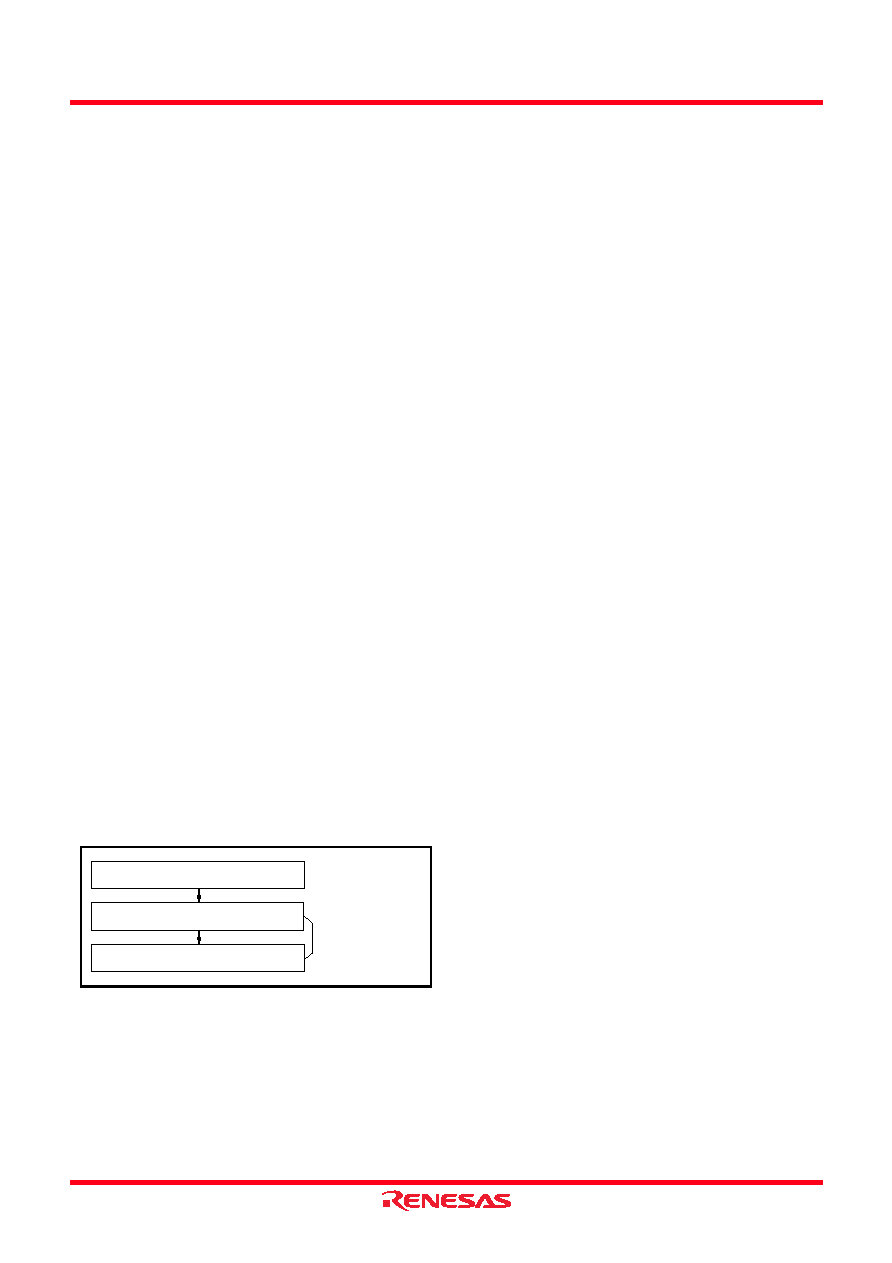
Fig. 104 Sequence of setting serial I/O1 control register
5. Pin Status After Transmission Completed
After transmission is completed, the TxD pin retains the level
when transmission is completed.
When the internal clock is selected in clock synchronous serial
I/O mode, the SCLK1 pin is set to “H”.
6. Serial I/O1 Enable Bit during Transmit Operation
During transmission, if the serial I/O1 enable bit (bit 7 of serial
I/O1 control register (address 001A16)) is set to “0”, the pin
function is set to an I/O port and the internal transmit operation
continues even though transmit data is not output externally.
Also, if the transmit buffer register is written in this state,
transmit operation starts internally. If the serial I/O1 enable bit is
set to “1” at this time, transmit data is output to the TxD pin from
that point.
7. Transmission
Control
When
External
Clock
Selected
During data transmission, if the external clock is selected as the
synchronous clock, set the transmit enable bit to “1” while SCLK1
is set to “H”. Also, write to the transmit buffer register while
SCLK1 is set to “H”.
8. Receive Operation in Clock Synchronous Serial I/O
Mode
During reception in clock synchronous serial I/O mode, set both
the transmit enable bit and the receive enable bit to “1”. Then
write dummy data to the transmit buffer register. When the
internal clock is selected as the synchronous clock, the
synchronous clock is output at this point and receive operation
starts. When the external clock is selected, reception is enabled at
this point and inputting the external clock starts transmit
operation.
The P41/TxD pin outputs dummy data written in the transmit
buffer register.
9. Transmit/Receive Operation in Clock Synchronous
Serial I/O Mode
In clock synchronous serial I/O mode, set the transmit enable bit
and the receive enable bit to “0” simultaneously to stop
transmit/receive operations. If only one of the operations is
stopped, transmission and reception cannot be synchronized,
which will cause a bit error.
Notes on Serial I/O2
1. Switching Synchronous Clock
If the synchronous clock is switched by the serial I/O2
synchronous clock selection bit (bit 6 of serial I/O2 control
register (address 001D16)), initialize the serial I/O2 counter
(writing to serial I/O2 register (address 001F16)).
2. Notes When External Clock Selected
When the external clock is selected as the synchronous clock, the
SOUT2 pin retains the D7 level after transfer is completed.
However, if the synchronous clock is continuously input, the
serial I/O2 register continues shifting and the SOUT2 pin keeps
outputting transmit data.
Also, write to the serial I/O2 register while SCLK2 is set to “H”.
When the internal clock is selected as the synchronous clock, the
SOUT2 pin is placed in the high-impedance state after transfer is
completed.
Set bits 0 to 3, and 6 of the serial I/O1 control
register.
Set both the transmit enable bit (TE) and the
receive enable bit (RE) to “0”
Set both the transmit enable bit (TE) and the receive
enable bit (RE), or one of them to “1”.
Settings can be made with
the LDM instruction at the
same time
相关PDF资料 |
PDF描述 |
|---|---|
| MC68B05P2L | 8-BIT, MROM, 2 MHz, MICROCONTROLLER, CDIP28 |
| MC908QB4MDT | 8-BIT, FLASH, 8 MHz, MICROCONTROLLER, PDSO16 |
| MC908QY2AVDWE | 8-BIT, FLASH, 8 MHz, MICROCONTROLLER, PDSO16 |
| MK2745-20SLF | 108 MHz, VIDEO CLOCK GENERATOR, PDSO16 |
| MK2742-04SLFTR | 81 MHz, VIDEO CLOCK GENERATOR, PDSO16 |
相关代理商/技术参数 |
参数描述 |
|---|---|
| M38D59GFFP#U0 | 功能描述:IC 740/38D5 MCU QZ-ROM 80QFP RoHS:是 类别:集成电路 (IC) >> 嵌入式 - 微控制器, 系列:740/38000 标准包装:250 系列:80C 核心处理器:8051 芯体尺寸:8-位 速度:16MHz 连通性:EBI/EMI,I²C,UART/USART 外围设备:POR,PWM,WDT 输入/输出数:40 程序存储器容量:- 程序存储器类型:ROMless EEPROM 大小:- RAM 容量:256 x 8 电压 - 电源 (Vcc/Vdd):4.5 V ~ 5.5 V 数据转换器:A/D 8x10b 振荡器型:内部 工作温度:-40°C ~ 85°C 封装/外壳:68-LCC(J 形引线) 包装:带卷 (TR) |
| M38D59GFHP#U0 | 功能描述:IC 740/38D5 MCU QZ-ROM 80LQFP RoHS:是 类别:集成电路 (IC) >> 嵌入式 - 微控制器, 系列:740/38000 标准包装:250 系列:80C 核心处理器:8051 芯体尺寸:8-位 速度:16MHz 连通性:EBI/EMI,I²C,UART/USART 外围设备:POR,PWM,WDT 输入/输出数:40 程序存储器容量:- 程序存储器类型:ROMless EEPROM 大小:- RAM 容量:256 x 8 电压 - 电源 (Vcc/Vdd):4.5 V ~ 5.5 V 数据转换器:A/D 8x10b 振荡器型:内部 工作温度:-40°C ~ 85°C 封装/外壳:68-LCC(J 形引线) 包装:带卷 (TR) |
| M38D59T-RLFS | 功能描述:BOARD EMULATOR FOR 38D5 GROUP RoHS:否 类别:编程器,开发系统 >> 内电路编程器、仿真器以及调试器 系列:- 产品变化通告:Development Systems Discontinuation 19/Jul/2010 标准包装:1 系列:* 类型:* 适用于相关产品:* 所含物品:* |
| M38DC-15 | 制造商:M/A-COM Technology Solutions 功能描述:MIXER(SPEC UX1015) - Bulk |
| M38K00F1-16FP | 制造商:MITSUBISHI 制造商全称:Mitsubishi Electric Semiconductor 功能描述:SINGLE-CHIP 8-BIT CMOS MICROCOMPUTER |
发布紧急采购,3分钟左右您将得到回复。