- 您现在的位置:买卖IC网 > PDF目录80499 > M38D59GC-XXXFP 8-BIT, MROM, 6.25 MHz, MICROCONTROLLER, PQFP80 PDF资料下载
参数资料
| 型号: | M38D59GC-XXXFP |
| 元件分类: | 微控制器/微处理器 |
| 英文描述: | 8-BIT, MROM, 6.25 MHz, MICROCONTROLLER, PQFP80 |
| 封装: | 14 X 20 MM, 0.80 MM PITCH, PLASTIC, QFP-80 |
| 文件页数: | 93/142页 |
| 文件大小: | 2004K |
| 代理商: | M38D59GC-XXXFP |
第1页第2页第3页第4页第5页第6页第7页第8页第9页第10页第11页第12页第13页第14页第15页第16页第17页第18页第19页第20页第21页第22页第23页第24页第25页第26页第27页第28页第29页第30页第31页第32页第33页第34页第35页第36页第37页第38页第39页第40页第41页第42页第43页第44页第45页第46页第47页第48页第49页第50页第51页第52页第53页第54页第55页第56页第57页第58页第59页第60页第61页第62页第63页第64页第65页第66页第67页第68页第69页第70页第71页第72页第73页第74页第75页第76页第77页第78页第79页第80页第81页第82页第83页第84页第85页第86页第87页第88页第89页第90页第91页第92页当前第93页第94页第95页第96页第97页第98页第99页第100页第101页第102页第103页第104页第105页第106页第107页第108页第109页第110页第111页第112页第113页第114页第115页第116页第117页第118页第119页第120页第121页第122页第123页第124页第125页第126页第127页第128页第129页第130页第131页第132页第133页第134页第135页第136页第137页第138页第139页第140页第141页第142页
Rev.3.04
May 20, 2008
REJ03B0158-0304
38D5 Group
Voltage Multiplier
The voltage multiplier performs threefold boosting. This circuit
inputs a reference voltage for boosting from LCD power input
pin VL1. Set each bit of the segment output disable registers and
the LCD mode registers in the following order for operating the
voltage multiplier.
(1) Set the segment output disable bits (bits 0 to 19) of the
segment output disable registers (SEG0, 1, 2) to “0” or “1”.
(2) Set the duty ratio selection bits (bits 0 to 2), the bias control
bit (bit 3), the LCD circuit divider division ratio selection
bits (bits 5 and 6), and the LCDCK count source selection
bit (bit 7) of the LCD mode register 1 to “0” or “1”.
(3) Set the VL3 connection bit (bit 1 of the LCD mode register 2
(LM2)) to “1”.
(4) Set the voltage multiplier control bit (bit0) of the LCD mode
register 2 to “1”.
When voltage is input to the VL1 pin during operating the voltage
multiplier, voltage that is twice as large as VL1 occurs at the VL2
pin, and voltage that is three times as large as VL1 occurs at the
VL3 pin.
The voltage multiplier is controlled by the voltage multiplier
control bit (bit 0 of the LCD mode register 2).
In addition, when the voltage multiplier is used, set the voltage
multiplier control bit to “1” (voltage multiplier enabled) after the
voltage 1.3 V or more and 2.1 V or less.
When the voltage multiplier is not used, set the VL3 connection
bit to “1” (open), and apply the suitable voltage for the power
supply input pins for LCD (VL1-VL3).
When VL3 connection bit is set to be open, VL3 pin is in a high
impedance state.
When the voltage multiplier is used, set the LCDCK frequency to
100 Hz or more. The on-chip oscillator cannot be used for
LCDCK.
In a system where the multiplier circuit is used (a multiplier
capacitor is externally connected between the C1 and C2 pins),
set the voltage multiplier circuit control bit to “1” (voltage
multiplier circuit enabled) before executing the STP or WIT
instruction.
Bias Control and Applied Voltage to LCD Power Input
Pins
Apply the voltage value shown in Table 13 according to the bias
value to the LCD power input pins. Apply the voltage value
shown in Table 13 according to the bias value by setting to VL3
connection bit (bit 1 of LCD mode register 1) to “1”, when the
voltage multiplier is not used.
Select a bias value by the bias control bit (bit 3 of the LCD mode
register 1).
NOTE:
1. VLCD is the maximum value of supplied voltage for the LCD
panel.
Common Pin and Duty Ratio Control
The common pins (COM0
COM7) to be used are determined by
duty ratio. Select duty ratio by the duty ratio selection bits (bits 0,
1 and 2 of the LCD mode register1). When reset is released, VCC
voltage is output from the common pin.
NOTE:
1. Unused common pin outputs the unselected waveform.
Segment Signal Output Pin
The segment signal output pins (SEG0
SEG31) are shared with
ports P0
P3. When these pins are used as the segment signal
output pins, set the direction registers of the corresponding pins
to “1”, and set the segment output disable register to “0”.
Also, these pins are set to the input port after reset, the VCC
voltage is output by the pull-up resistor.
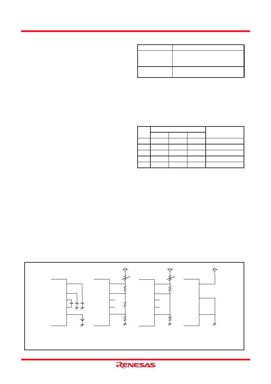
Fig. 45 Example of circuit at each bias (at external power supply input)
Table 13
Bias control and applied voltage to VL1
VL3
Bias value
Voltage value
1/3 bias
VL3 = VLCD
VL2 = 2/3 VLCD
VL1 = 1/3 VLCD
1/2 bias
VL3 = VLCD
VL2 = VL1 = 1/2 VLCD
Table 14
Duty ratio control and common pins used
Duty
ratio
Duty ratio selection bits
Common pins used
Bit 2
Bit 1
Bit 0
10
0
COM0
20
0
1
COM0, COM1
30
1
0
COM0
COM2
40
1
COM0
COM3
81
1
COM0
COM7
R4
R5
R4 = R5
1/2 bias
Contrast adjust
R1
R2
R3
1/3 bias
Voltage multiplier is not used.
VL1
VL3
VL2
*
P71/INT11
P70/INT01
VL1
VL3
VL2
*
P71/INT11
P70/INT01
1/3 bias: R1 = R2 = R3
1/3 bias
Voltage multiplier is used.
VL1
VL3
VL2
C2
C1
1/1 bias (static)
VL1
VL3
VL2
Contrast adjust
* : When the voltage multiplier is not used, the C1 and C2 pins function as input ports P70/INT01, P71/INT11.
相关PDF资料 |
PDF描述 |
|---|---|
| MC68B05P2L | 8-BIT, MROM, 2 MHz, MICROCONTROLLER, CDIP28 |
| MC908QB4MDT | 8-BIT, FLASH, 8 MHz, MICROCONTROLLER, PDSO16 |
| MC908QY2AVDWE | 8-BIT, FLASH, 8 MHz, MICROCONTROLLER, PDSO16 |
| MK2745-20SLF | 108 MHz, VIDEO CLOCK GENERATOR, PDSO16 |
| MK2742-04SLFTR | 81 MHz, VIDEO CLOCK GENERATOR, PDSO16 |
相关代理商/技术参数 |
参数描述 |
|---|---|
| M38D59GFFP#U0 | 功能描述:IC 740/38D5 MCU QZ-ROM 80QFP RoHS:是 类别:集成电路 (IC) >> 嵌入式 - 微控制器, 系列:740/38000 标准包装:250 系列:80C 核心处理器:8051 芯体尺寸:8-位 速度:16MHz 连通性:EBI/EMI,I²C,UART/USART 外围设备:POR,PWM,WDT 输入/输出数:40 程序存储器容量:- 程序存储器类型:ROMless EEPROM 大小:- RAM 容量:256 x 8 电压 - 电源 (Vcc/Vdd):4.5 V ~ 5.5 V 数据转换器:A/D 8x10b 振荡器型:内部 工作温度:-40°C ~ 85°C 封装/外壳:68-LCC(J 形引线) 包装:带卷 (TR) |
| M38D59GFHP#U0 | 功能描述:IC 740/38D5 MCU QZ-ROM 80LQFP RoHS:是 类别:集成电路 (IC) >> 嵌入式 - 微控制器, 系列:740/38000 标准包装:250 系列:80C 核心处理器:8051 芯体尺寸:8-位 速度:16MHz 连通性:EBI/EMI,I²C,UART/USART 外围设备:POR,PWM,WDT 输入/输出数:40 程序存储器容量:- 程序存储器类型:ROMless EEPROM 大小:- RAM 容量:256 x 8 电压 - 电源 (Vcc/Vdd):4.5 V ~ 5.5 V 数据转换器:A/D 8x10b 振荡器型:内部 工作温度:-40°C ~ 85°C 封装/外壳:68-LCC(J 形引线) 包装:带卷 (TR) |
| M38D59T-RLFS | 功能描述:BOARD EMULATOR FOR 38D5 GROUP RoHS:否 类别:编程器,开发系统 >> 内电路编程器、仿真器以及调试器 系列:- 产品变化通告:Development Systems Discontinuation 19/Jul/2010 标准包装:1 系列:* 类型:* 适用于相关产品:* 所含物品:* |
| M38DC-15 | 制造商:M/A-COM Technology Solutions 功能描述:MIXER(SPEC UX1015) - Bulk |
| M38K00F1-16FP | 制造商:MITSUBISHI 制造商全称:Mitsubishi Electric Semiconductor 功能描述:SINGLE-CHIP 8-BIT CMOS MICROCOMPUTER |
发布紧急采购,3分钟左右您将得到回复。