- 您现在的位置:买卖IC网 > PDF目录4100 > MC68EC060RC50 (Freescale Semiconductor)IC MPU 32BIT 50MHZ 206-PGA PDF资料下载
参数资料
| 型号: | MC68EC060RC50 |
| 厂商: | Freescale Semiconductor |
| 文件页数: | 117/128页 |
| 文件大小: | 0K |
| 描述: | IC MPU 32BIT 50MHZ 206-PGA |
| 标准包装: | 10 |
| 系列: | M680x0 |
| 处理器类型: | M680x0 32-位 |
| 速度: | 50MHz |
| 电压: | 3.3V |
| 安装类型: | 通孔 |
| 封装/外壳: | 206-BEPGA |
| 供应商设备封装: | 206-PGA(47.25x47.25) |
| 包装: | 托盘 |
第1页第2页第3页第4页第5页第6页第7页第8页第9页第10页第11页第12页第13页第14页第15页第16页第17页第18页第19页第20页第21页第22页第23页第24页第25页第26页第27页第28页第29页第30页第31页第32页第33页第34页第35页第36页第37页第38页第39页第40页第41页第42页第43页第44页第45页第46页第47页第48页第49页第50页第51页第52页第53页第54页第55页第56页第57页第58页第59页第60页第61页第62页第63页第64页第65页第66页第67页第68页第69页第70页第71页第72页第73页第74页第75页第76页第77页第78页第79页第80页第81页第82页第83页第84页第85页第86页第87页第88页第89页第90页第91页第92页第93页第94页第95页第96页第97页第98页第99页第100页第101页第102页第103页第104页第105页第106页第107页第108页第109页第110页第111页第112页第113页第114页第115页第116页当前第117页第118页第119页第120页第121页第122页第123页第124页第125页第126页第127页第128页
Memory Management Unit
4-20
M68060 USER’S MANUAL
MOTOROLA
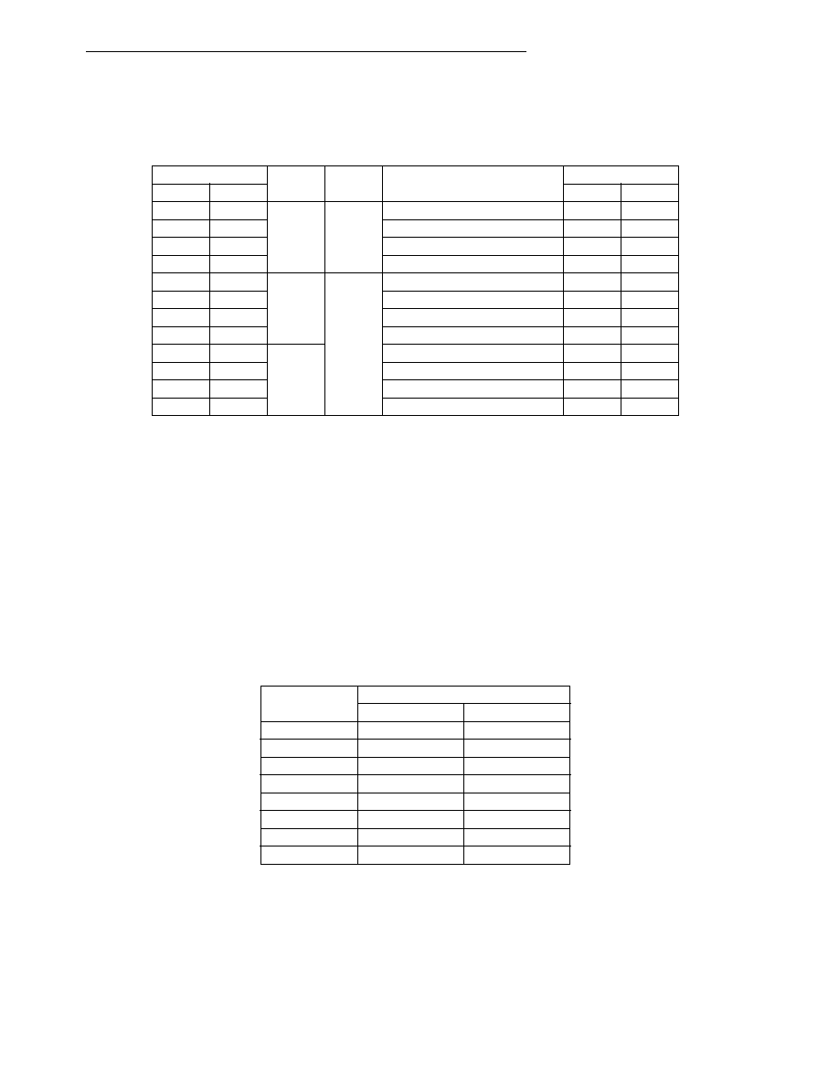
updated before the MC68060 allows a page to be accessed. Table 4-1 lists the page
descriptor update operations for each combination of U-bit, M-bit, write-protected, and read
or write access type.
An alternate address space access is a special case that is immediately used as a physical
address without translation. Because the MC68060 implements a merged instruction and
data space, instruction address spaces (SFC/DFC = $6 or $2) using the MOVES instruction
are converted into data references (SFC/DFC = $5 or $1). The data memory unit handles
these translated accesses as normal data accesses. If the access fails due to an ATC fault
or a physical bus error, the resulting access error stack frame contains the converted func-
tion code in the TM field for the faulted access. If the MOVES instruction is used to write
instruction address space, then to maintain cache coherency, the corresponding addresses
must be invalidated in the instruction cache. The SFC and DFC values and results for nor-
mal (TT = 0) and for MOVES (TT = 10) accesses are listed in Table 4-2.
4.2.6 Address Translation Protection
The MC68060 MMUs provide separate translation tables for supervisor and user address
spaces. The translation tables contain both mapping and protection information. Each table
and page descriptor includes a write-protect (W) bit that can be set to provide write protec-
Table 4-1. Updating U-Bit and M-Bit for Page Descriptors
Previous Status
WP Bit
Access
Type
Page Descriptor
Update Operation
New Status
U-Bit
M-Bit
U-Bit
M-Bit
00
X
Read
Locked RMW Access to Set U
1
0
1
Locked RMW Access to Set U
1
0
None
1
0
1
None
1
00
0
Write
Write to Set U and M
1
0
1
Write to Set U
1
0
Write to Set M
1
None
1
00
1
None
0
1
None
0
1
0
None
1
0
1
None
1
NOTE: WP indicates the accumulated write-protect status.
Table 4-2. SFC and DFC Values
SFC/DFC Value
Results
TT
TM
000
10
000
001
00
001
010
00
001
011
10
011
100
10
100
101
00
101
110
00
101
111
10
111
相关PDF资料 |
PDF描述 |
|---|---|
| IDT71V65803S133BGG8 | IC SRAM 9MBIT 133MHZ 119BGA |
| MPC8270ZUUPEA | IC MPU POWERQUICC II 480-TBGA |
| IDT71V65803S133BG8 | IC SRAM 9MBIT 133MHZ 119BGA |
| MPC860PCZQ66D4 | IC MPU PWRQUICC 66MHZ 357-PBGA |
| IDT71V65803S100BGG8 | IC SRAM 9MBIT 100MHZ 119BGA |
相关代理商/技术参数 |
参数描述 |
|---|---|
| MC68EC060RC66 | 功能描述:微处理器 - MPU 32B W/ CACHE RoHS:否 制造商:Atmel 处理器系列:SAMA5D31 核心:ARM Cortex A5 数据总线宽度:32 bit 最大时钟频率:536 MHz 程序存储器大小:32 KB 数据 RAM 大小:128 KB 接口类型:CAN, Ethernet, LIN, SPI,TWI, UART, USB 工作电源电压:1.8 V to 3.3 V 最大工作温度:+ 85 C 安装风格:SMD/SMT 封装 / 箱体:FBGA-324 |
| MC68EC060RC75 | 功能描述:微处理器 - MPU 32B W/ CACHE RoHS:否 制造商:Atmel 处理器系列:SAMA5D31 核心:ARM Cortex A5 数据总线宽度:32 bit 最大时钟频率:536 MHz 程序存储器大小:32 KB 数据 RAM 大小:128 KB 接口类型:CAN, Ethernet, LIN, SPI,TWI, UART, USB 工作电源电压:1.8 V to 3.3 V 最大工作温度:+ 85 C 安装风格:SMD/SMT 封装 / 箱体:FBGA-324 |
| MC68EC060ZU50 | 功能描述:IC MPU 68K 50MHZ 304-TBGA RoHS:否 类别:集成电路 (IC) >> 嵌入式 - 微处理器 系列:M680x0 标准包装:1 系列:MPC85xx 处理器类型:32-位 MPC85xx PowerQUICC III 特点:- 速度:1.2GHz 电压:1.1V 安装类型:表面贴装 封装/外壳:783-BBGA,FCBGA 供应商设备封装:783-FCPBGA(29x29) 包装:托盘 |
| MC68EC060ZU66 | 功能描述:微处理器 - MPU 32B W/ CACHE RoHS:否 制造商:Atmel 处理器系列:SAMA5D31 核心:ARM Cortex A5 数据总线宽度:32 bit 最大时钟频率:536 MHz 程序存储器大小:32 KB 数据 RAM 大小:128 KB 接口类型:CAN, Ethernet, LIN, SPI,TWI, UART, USB 工作电源电压:1.8 V to 3.3 V 最大工作温度:+ 85 C 安装风格:SMD/SMT 封装 / 箱体:FBGA-324 |
| MC68EC060ZU75 | 功能描述:微处理器 - MPU 32B W/ CACHE RoHS:否 制造商:Atmel 处理器系列:SAMA5D31 核心:ARM Cortex A5 数据总线宽度:32 bit 最大时钟频率:536 MHz 程序存储器大小:32 KB 数据 RAM 大小:128 KB 接口类型:CAN, Ethernet, LIN, SPI,TWI, UART, USB 工作电源电压:1.8 V to 3.3 V 最大工作温度:+ 85 C 安装风格:SMD/SMT 封装 / 箱体:FBGA-324 |
发布紧急采购,3分钟左右您将得到回复。