- 您现在的位置:买卖IC网 > PDF目录69032 > MCM16Y1BACFT16 (MOTOROLA INC) 16-BIT, MROM, MICROCONTROLLER, PQFP160 PDF资料下载
参数资料
| 型号: | MCM16Y1BACFT16 |
| 厂商: | MOTOROLA INC |
| 元件分类: | 微控制器/微处理器 |
| 英文描述: | 16-BIT, MROM, MICROCONTROLLER, PQFP160 |
| 封装: | QFP-160 |
| 文件页数: | 82/138页 |
| 文件大小: | 784K |
| 代理商: | MCM16Y1BACFT16 |
第1页第2页第3页第4页第5页第6页第7页第8页第9页第10页第11页第12页第13页第14页第15页第16页第17页第18页第19页第20页第21页第22页第23页第24页第25页第26页第27页第28页第29页第30页第31页第32页第33页第34页第35页第36页第37页第38页第39页第40页第41页第42页第43页第44页第45页第46页第47页第48页第49页第50页第51页第52页第53页第54页第55页第56页第57页第58页第59页第60页第61页第62页第63页第64页第65页第66页第67页第68页第69页第70页第71页第72页第73页第74页第75页第76页第77页第78页第79页第80页第81页当前第82页第83页第84页第85页第86页第87页第88页第89页第90页第91页第92页第93页第94页第95页第96页第97页第98页第99页第100页第101页第102页第103页第104页第105页第106页第107页第108页第109页第110页第111页第112页第113页第114页第115页第116页第117页第118页第119页第120页第121页第122页第123页第124页第125页第126页第127页第128页第129页第130页第131页第132页第133页第134页第135页第136页第137页第138页
MOTOROLA
MC68HC16Y1
48
MC68HC16Y1TS/D
size signals indicate the number of bytes remaining to be transferred during an operand cycle. They are
valid while the address strobe (AS) is asserted. The table below shows SIZ0 and SIZ1 encoding. The
read/write (R/W) signal determines the direction of the transfer during a bus cycle. This signal changes
state, when required, at the beginning of a bus cycle, and is valid while AS is asserted. R/W only tran-
sitions when a write cycle is preceded by a read cycle or vice versa. The signal may remain low for two
consecutive write cycles.
3.5.2 Function Codes
Function code signals FC[2:0] are automatically generated by the CPU16. The function codes can be
considered address extensions that automatically select one of eight address spaces to which an ad-
dress applies. These spaces are designated as either user or supervisor, and program or data spaces.
Because the CPU16 always operates in supervisor mode (FC2 always = 1), address spaces 0 to 3 are
not used. Address space 7 is designated CPU space. CPU space is used for control information not
normally associated with read or write bus cycles. Function codes are valid while AS is asserted.
3.5.3 Address Bus
Address bus signals ADDR[19:0] define the address of the most significant byte to be transferred during
a bus cycle. The MCU places the address on the bus at the beginning of a bus cycle. The address is
valid while AS is asserted. Because the CPU16 in the MC68HC16Y1 does not drive ADDR[23:20],
these lines follow the logic state of ADDR19.
3.5.4 Address Strobe
AS is a timing signal that indicates the validity of an address on the address bus and of many control
signals. It is asserted one-half clock after the beginning of a bus cycle.
3.5.5 Data Bus
Data bus signals DATA[15:0] comprise a bidirectional, non-multiplexed parallel bus that transfers data
to or from the MCU. A read or write operation can transfer 8 or 16 bits of data in one bus cycle. During
a read cycle, the data is latched by the MCU on the last falling edge of the clock for that bus cycle. For
a write cycle, all 16 bits of the data bus are driven, regardless of the port width or operand size. The
MCU places the data on the data bus one-half clock cycle after AS is asserted in a write cycle.
3.5.6 Data Strobe
Data strobe (DS) is a timing signal. For a read cycle, the MCU asserts DS to signal an external device
to place data on the bus. DS is asserted at the same time as AS during a read cycle. For a write cycle,
DS signals an external device that data on the bus is valid. The MCU asserts DS one full clock cycle
after the assertion of AS during a write cycle.
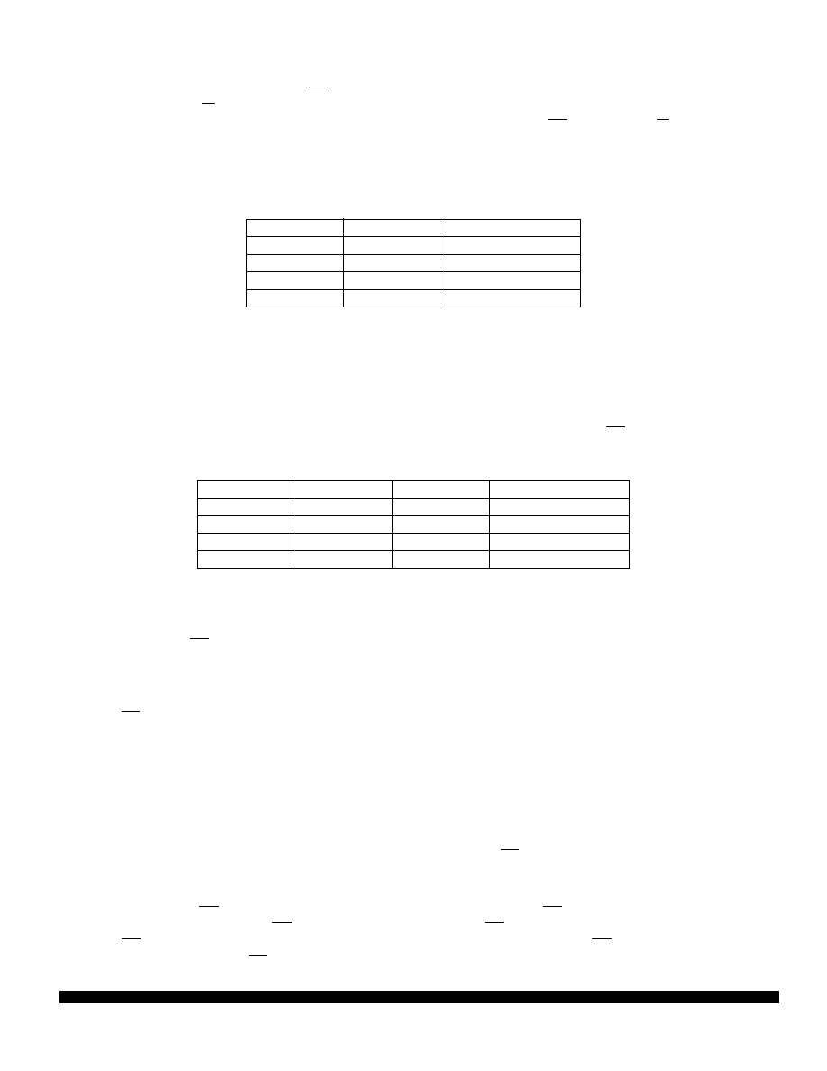
Table 13 Size Signal Encoding
SIZ1
SIZ0
Transfer Size
0
1
Byte
1
0
Word
1
3 Byte
0
Long Word
Table 14 CPU16 Address Space Encoding
FC2
FC1
FC0
Address Space
1
0
Reserved
1
0
1
Data Space
1
0
Program Space
1
CPU Space
相关PDF资料 |
PDF描述 |
|---|---|
| MCM16Y1BGCFT16 | 16-BIT, MROM, MICROCONTROLLER, PQFP160 |
| M68HC16Y1CFC | 16-BIT, MROM, MICROCONTROLLER, PQFP16 |
| MCV14AI/SL | 8-BIT, FLASH, 20 MHz, RISC MICROCONTROLLER, PDSO14 |
| MCV14ATI/SL | 8-BIT, FLASH, 20 MHz, RISC MICROCONTROLLER, PDSO14 |
| MCV14AI/P | 8-BIT, FLASH, 20 MHz, RISC MICROCONTROLLER, PDIP14 |
相关代理商/技术参数 |
参数描述 |
|---|---|
| MCM16Z2BCFC16 | 制造商:FREESCALE 制造商全称:Freescale Semiconductor, Inc 功能描述:Symbols and Operators, CPU16 Register Mnemonics |
| MCM16Z2BCFC16B1 | 制造商:FREESCALE 制造商全称:Freescale Semiconductor, Inc 功能描述:Symbols and Operators, CPU16 Register Mnemonics |
| MCM16Z2BCFC20 | 制造商:FREESCALE 制造商全称:Freescale Semiconductor, Inc 功能描述:Symbols and Operators, CPU16 Register Mnemonics |
| MCM16Z2BCFC20B1 | 制造商:FREESCALE 制造商全称:Freescale Semiconductor, Inc 功能描述:M68HC16Z Series users manual |
| MCM16Z2BCFC25 | 制造商:FREESCALE 制造商全称:Freescale Semiconductor, Inc 功能描述:M68HC16Z Series users manual |
发布紧急采购,3分钟左右您将得到回复。