- 您现在的位置:买卖IC网 > PDF目录385639 > MT28C3224P20 (Micron Technology, Inc.) FLASH AND SRAM COMBO MEMORY PDF资料下载
参数资料
| 型号: | MT28C3224P20 |
| 厂商: | Micron Technology, Inc. |
| 元件分类: | DRAM |
| 英文描述: | FLASH AND SRAM COMBO MEMORY |
| 中文描述: | 闪存和SRAM式内存 |
| 文件页数: | 12/42页 |
| 文件大小: | 498K |
| 代理商: | MT28C3224P20 |
第1页第2页第3页第4页第5页第6页第7页第8页第9页第10页第11页当前第12页第13页第14页第15页第16页第17页第18页第19页第20页第21页第22页第23页第24页第25页第26页第27页第28页第29页第30页第31页第32页第33页第34页第35页第36页第37页第38页第39页第40页第41页第42页
F
12
2 Meg x 16 Page Flash 256K x 16 SRAM Combo Memory
MT28C3224P20_3.p65 – Rev. 3, Pub. 7/02
Micron Technology, Inc., reserves the right to change products or specifications without notice.
2002, Micron Technology, Inc.
2 MEG x 16 PAGE FLASH
256K x 16 SRAM COMBO MEMORY
ADVANCE
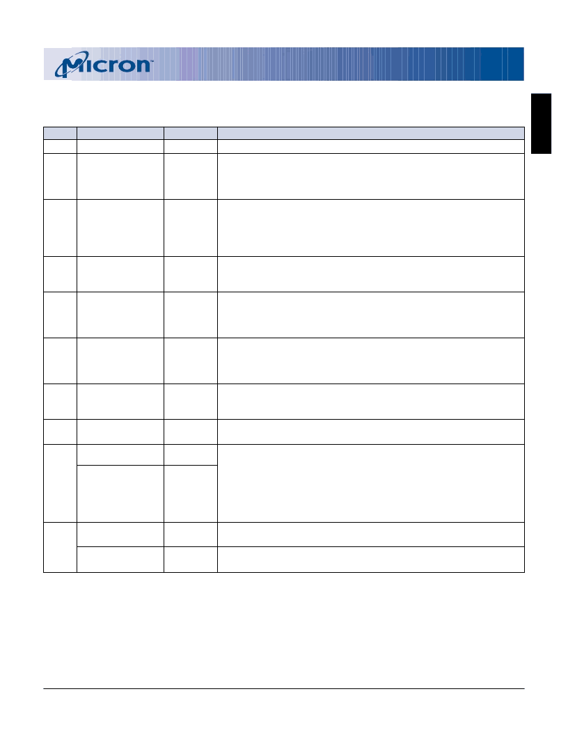
Table 5
Command Descriptions
CODE DEVICE MODE
10h
Alt. Program Setup
20h
Erase Setup
BUS CYCLE
First
First
DESCRIPTION
Operates the same as a PROGRAM SETUP command.
Prepares the CSM for an ERASE CONFIRM command. If the next
command is not an ERASE CONFIRM command, the command will
be ignored, and the device will go to read status mode and wait for
another command.
A two-cycle command: The first cycle prepares for a PROGRAM
operation, the second cycle latches addresses and data and initiates
the WSM to execute the program algorithm. The Flash outputs status
register data on the falling edge of F_OE# or F_CE#, whichever
occurs first.
The WSM can set the program status (SR4), and erase status (SR5) bits
in the status register to “1,” but it cannot clear them to “0.” Issuing
this command clears those bits to “0.”
Prepares the CSM for changes to the block locking status. If the next
command is not BLOCK UNLOCK, BLOCK LOCK or BLOCK LOCK
DOWN, the command will be ignored, and the device will go to read
status mode.
Places the device into read status register mode. Reading the device
outputs the contents of the status register for the addressed bank.
The device automatically enters this mode for the addressed bank
after a PROGRAM or ERASE operation has been initiated.
Puts the device into the read protection configuration mode so that
reading the device outputs the manufacturer/device codes or block
lock status.
Puts the device into the read query mode so that reading the device
outputs common Flash interface information.
Suspends the currently executing PROGRAM/ERASE operation. The
status register indicates when the operation has been successfully
suspended by setting either the program suspend (SR2) or erase
suspend (SR6) and the WSMS bit (SR7) to a “1” (ready). The WSM
continues to idle in the suspend state, regardless of the state of all
input control pins except F_RP#, which immediately shuts down the
WSM and the remainder of the chip if F_RP# is driven to V
IL
.
Writes a specific code into the device protection register.
40h
Program Setup
First
50h
Clear Status
Register
First
60h
Protection
Configuration
Setup
First
70h
Read Status
Register
First
90h
Read Protection
Configuration
First
98h
Read Query
First
B0h
Program Suspend
First
Erase Suspend
First
C0h
Program Device
Protection Register
Lock Device
Protection Register
First
First
Locks the device protection register; data can no longer be changed.
(continued on the next page)
相关PDF资料 |
PDF描述 |
|---|---|
| MT28F200B3 | FLASH MEMORY |
| MT28F200B5 | FLASH MEMORY |
| MT28F320A18 | FLASH MEMORY |
| MT2D18 | 1 Meg x 8 DRAM Module(5V,1M x 8 动态RAM模块) |
| MT46V16M4 | 4 Meg x 4 x 4 banks DDR SDRAM(4 M x 4 x 4组,双数据速率同步动态RAM) |
相关代理商/技术参数 |
参数描述 |
|---|---|
| MT28C3224P20FL-80 BET | 制造商:Micron Technology Inc 功能描述: |
| MT28C3224P20FL-80 BET TR | 制造商:Micron Technology Inc 功能描述: |
| MT28C6428P18 | 制造商:MICRON 制造商全称:Micron Technology 功能描述:FLASH AND SRAM COMBO MEMORY |
| MT28C6428P18FM-85 BET | 制造商:Micron Technology Inc 功能描述: |
| MT28C6428P18FM-85 BET TR | 制造商:Micron Technology Inc 功能描述: |
发布紧急采购,3分钟左右您将得到回复。