- 您现在的位置:买卖IC网 > PDF目录385639 > MT28C3224P20 (Micron Technology, Inc.) FLASH AND SRAM COMBO MEMORY PDF资料下载
参数资料
| 型号: | MT28C3224P20 |
| 厂商: | Micron Technology, Inc. |
| 元件分类: | DRAM |
| 英文描述: | FLASH AND SRAM COMBO MEMORY |
| 中文描述: | 闪存和SRAM式内存 |
| 文件页数: | 34/42页 |
| 文件大小: | 498K |
| 代理商: | MT28C3224P20 |
第1页第2页第3页第4页第5页第6页第7页第8页第9页第10页第11页第12页第13页第14页第15页第16页第17页第18页第19页第20页第21页第22页第23页第24页第25页第26页第27页第28页第29页第30页第31页第32页第33页当前第34页第35页第36页第37页第38页第39页第40页第41页第42页
F
34
2 Meg x 16 Page Flash 256K x 16 SRAM Combo Memory
MT28C3224P20_3.p65 – Rev. 3, Pub. 7/02
Micron Technology, Inc., reserves the right to change products or specifications without notice.
2002, Micron Technology, Inc.
2 MEG x 16 PAGE FLASH
256K x 16 SRAM COMBO MEMORY
ADVANCE
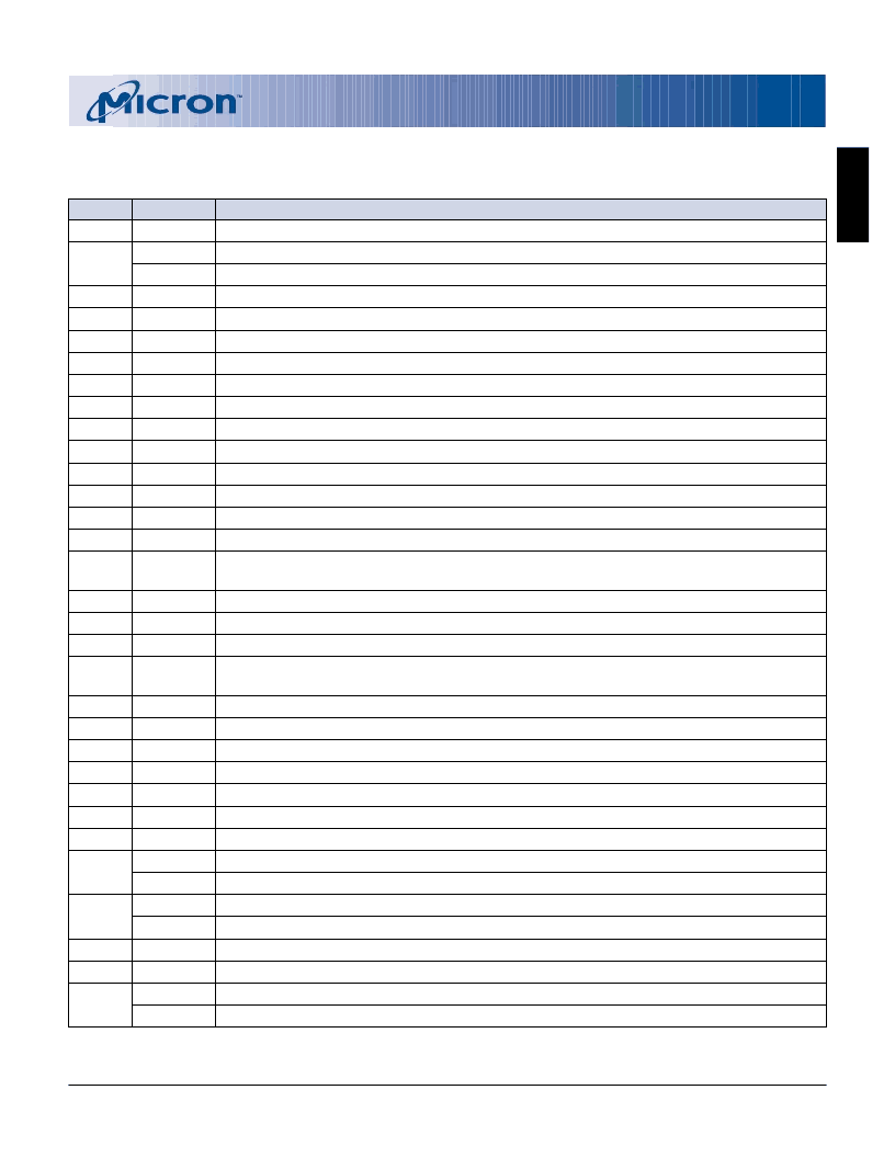
Table 11
CFI
OFFSET
00
01
DATA
2Ch
B4h
B5h
reserved
0051,0052
0059
0003, 0000
0039, 0000
0000, 0000
0000, 0000
0017
0022
00B4
00C6
0003
0000
DESCRIPTION
Manufacturer Code
Top boot block device code
Bottom boot block device code
Reserved
“QR”
“Y”
Primary OEM command set
Address for primary extended table
Alternate OEM command set
Address for OEM extended table
V
CC
MIN for Erase/Write; Bit7–Bit4 Volts in BCD; Bit3–Bit0 100mV in BCD
V
CC
MAX for Erase/Write; Bit7–Bit4 Volts in BCD; Bit3–Bit0 100mV in BCD
V
PP
MIN for Erase/Write; Bit7–Bit4 Volts in Hex; Bit3–Bit0 100mV in BCD
V
PP
MAX for Erase/Write; Bit7–Bit4 Volts in Hex; Bit3–Bit0 100mV in BCD
Typical timeout for single byte/word program, 2
n
μs, 0000 = not supported
Typical timeout for maximum size multiple byte/word program, 2
n
μs, 0000 = not
supported
Typical timeout for individual block erase, 2
n
ms, 0000 = not supported
Typical timeout for full chip erase, 2
n
ms, 0000 = not supported
Maximum timeout for single byte/word program, 2
n
μs, 0000 = not supported
Maximum timeout for maximum size multiple byte/word program, 2
n
μs, 0000 = not
supported
Maximum timeout for individual block erase, 2
n
ms, 0000 = not supported
Maximum timeout for full chip erase, 2
n
ms, 0000 = not supported
Device size, 2
n
bytes
Bus interface x8 = 0, x16 = 1, x8/x16 = 2
Flash device interface description 0000 = async
Maximum number of bytes in multi-byte program or page, 2
n
Number of erase block regions within device (4K words and 32K words)
Top boot block device erase block region information 1, 8 blocks …
Bottom boot block device erase block region information 1, 8 blocks …
Erase block region information 1, 8 blocks …
…of 8KB
7 blocks of ….
……64KB
Top boot block device ……48 blocks of
Bottom boot block device ……48 blocks of
02–0F
10, 11
12
13, 14
15, 16
17, 18
19, 1A
1B
1C
1D
1E
1F
20
21
22
23
24
0009
0000
000C
0000
25
26
27
28
29
0003
0000
0016
0001
0000
2A, 2B
2C
2D, 2E
0000, 0000
0003
002F, 0000
0007, 0000
0000, 0001
0020, 0000
000E, 0000
0000, 0001
0007, 0000
002F, 0000
2F, 30
31, 32
33, 34
35, 36
(continued on the next page)
相关PDF资料 |
PDF描述 |
|---|---|
| MT28F200B3 | FLASH MEMORY |
| MT28F200B5 | FLASH MEMORY |
| MT28F320A18 | FLASH MEMORY |
| MT2D18 | 1 Meg x 8 DRAM Module(5V,1M x 8 动态RAM模块) |
| MT46V16M4 | 4 Meg x 4 x 4 banks DDR SDRAM(4 M x 4 x 4组,双数据速率同步动态RAM) |
相关代理商/技术参数 |
参数描述 |
|---|---|
| MT28C3224P20FL-80 BET | 制造商:Micron Technology Inc 功能描述: |
| MT28C3224P20FL-80 BET TR | 制造商:Micron Technology Inc 功能描述: |
| MT28C6428P18 | 制造商:MICRON 制造商全称:Micron Technology 功能描述:FLASH AND SRAM COMBO MEMORY |
| MT28C6428P18FM-85 BET | 制造商:Micron Technology Inc 功能描述: |
| MT28C6428P18FM-85 BET TR | 制造商:Micron Technology Inc 功能描述: |
发布紧急采购,3分钟左右您将得到回复。