- 您现在的位置:买卖IC网 > PDF目录385639 > MT28C3224P20 (Micron Technology, Inc.) FLASH AND SRAM COMBO MEMORY PDF资料下载
参数资料
| 型号: | MT28C3224P20 |
| 厂商: | Micron Technology, Inc. |
| 元件分类: | DRAM |
| 英文描述: | FLASH AND SRAM COMBO MEMORY |
| 中文描述: | 闪存和SRAM式内存 |
| 文件页数: | 22/42页 |
| 文件大小: | 498K |
| 代理商: | MT28C3224P20 |
第1页第2页第3页第4页第5页第6页第7页第8页第9页第10页第11页第12页第13页第14页第15页第16页第17页第18页第19页第20页第21页当前第22页第23页第24页第25页第26页第27页第28页第29页第30页第31页第32页第33页第34页第35页第36页第37页第38页第39页第40页第41页第42页

F
22
2 Meg x 16 Page Flash 256K x 16 SRAM Combo Memory
MT28C3224P20_3.p65 – Rev. 3, Pub. 7/02
Micron Technology, Inc., reserves the right to change products or specifications without notice.
2002, Micron Technology, Inc.
2 MEG x 16 PAGE FLASH
256K x 16 SRAM COMBO MEMORY
ADVANCE
The LOCK DOWN function is dependent on the
F_WP# input. When F_WP# = 0, blocks in lock down
[011] are protected from program, erase, and lock sta-
tus changes. When F_WP# = 1, the LOCK DOWN func-
tion is disabled ([111]) and locked down blocks can be
individually unlocked by a software command to the
[110] state, where they can be erased and programmed.
These blocks can then be relocked [111] and unlocked
[110], as desired, as long as F_WP# remains HIGH.
When F_WP# goes LOW, blocks that were previously
locked down return to the lock down state [011] regard-
less of any changes made while F_WP# was HIGH. De-
vice reset or power-down resets all locks, including
those in lock down, to the locked state (see Table 9).
READING A BLOCK’S LOCK STATUS
The lock status of every block can be read in the
read device identification mode. To enter this mode,
write 90h to the bank containing address 00h. Subse-
quent READs at block address +00002 will output the
lock status of that block. The lowest two outputs, DQ0
and DQ1, represent the lock status. DQ0 indicates the
block lock/unlock status and is set by the LOCK com-
mand and cleared by the UNLOCK command. It is also
automatically set when entering lock down. DQ1 indi-
cates lock down status and is set by the LOCK DOWN
command. It can only be cleared by reset or power-
down, not by software. Table 8 shows the block locking
state transition scheme. After data is read from the
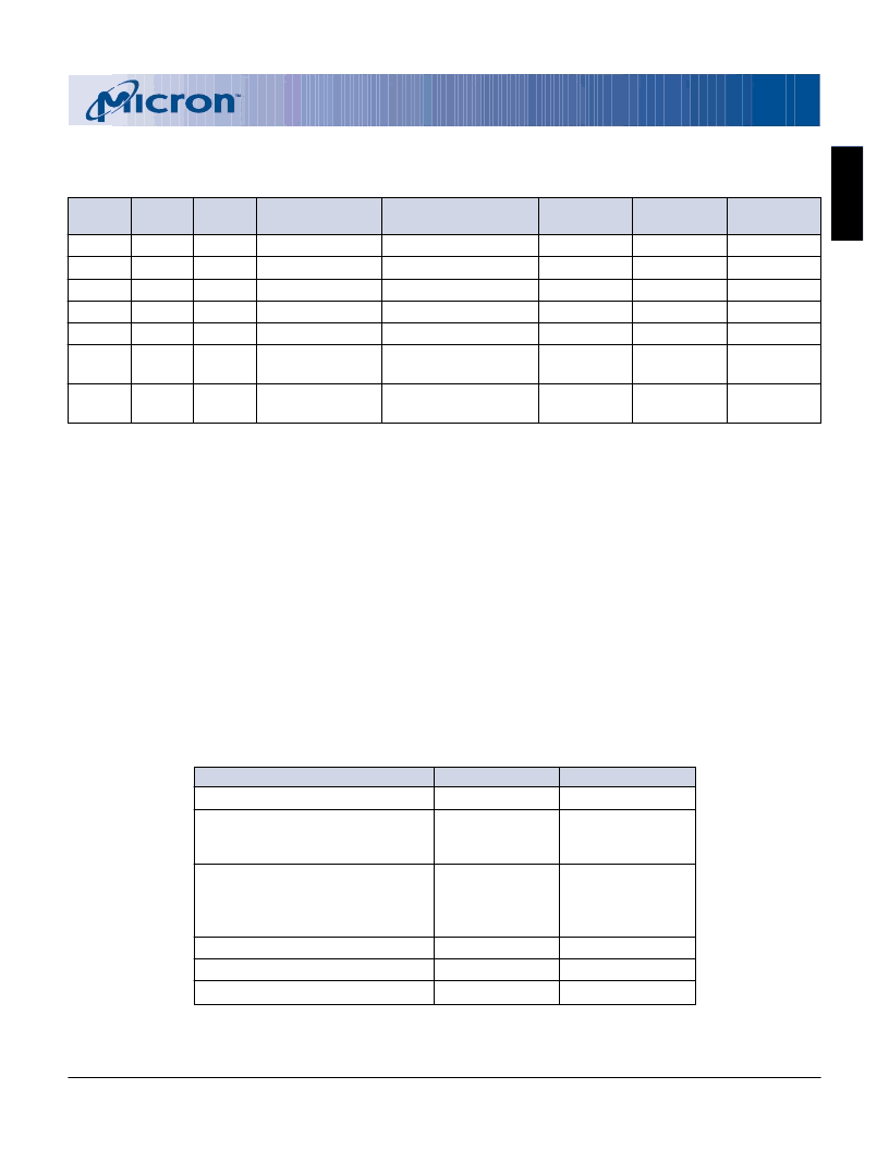
Table 8
Block Locking State Transition
ERASE/PROGRAM
ALLOWED
Yes
No
No
Yes
No
Yes
LOCK
DOWN
To [011]
To [011]
–
To [111]
To [111]
To [111]
F_WP#
0
0
0
1
1
1
DQ1
0
0
1
0
0
1
DQ0
0
1
1
0
1
0
NAME
Unlocked
Locked (Default)
Lock Down
Unlocked
Locked
Lock Down
Disabled
Lock Down
Disabled
LOCK
To [001]
–
–
To [101]
–
To [111]
UNLOCK
–
To [000]
–
–
To [100]
–
1
1
1
No
–
To [110]
–
ITEM
Manufacturer Code (x16)
Device Code
·
Top boot configuration
·
Bottom boot configuration
Block Lock Configuration
·
Block is unlocked
·
Block is locked
·
Block is locked down
Chip Protection Register Lock
Chip Protection Register 1
Chip Protection Register 2
ADDRESS
2
00000h
00001h
DATA
002Ch
44B4h
44B5h
Lock
DQ0 = 0
DQ0 = 1
DQ1 = 1
PR Lock
Factory Data
User Data
XX002h
80h
81h–84h
85h–88h
NOTE:
1. Other locations within the configuration address space are reserved by
Micron for future use.
2. “XX” specifies the block address of lock configuration.
Table 9
Chip Configuration Addressing
1
相关PDF资料 |
PDF描述 |
|---|---|
| MT28F200B3 | FLASH MEMORY |
| MT28F200B5 | FLASH MEMORY |
| MT28F320A18 | FLASH MEMORY |
| MT2D18 | 1 Meg x 8 DRAM Module(5V,1M x 8 动态RAM模块) |
| MT46V16M4 | 4 Meg x 4 x 4 banks DDR SDRAM(4 M x 4 x 4组,双数据速率同步动态RAM) |
相关代理商/技术参数 |
参数描述 |
|---|---|
| MT28C3224P20FL-80 BET | 制造商:Micron Technology Inc 功能描述: |
| MT28C3224P20FL-80 BET TR | 制造商:Micron Technology Inc 功能描述: |
| MT28C6428P18 | 制造商:MICRON 制造商全称:Micron Technology 功能描述:FLASH AND SRAM COMBO MEMORY |
| MT28C6428P18FM-85 BET | 制造商:Micron Technology Inc 功能描述: |
| MT28C6428P18FM-85 BET TR | 制造商:Micron Technology Inc 功能描述: |
发布紧急采购,3分钟左右您将得到回复。