- 您现在的位置:买卖IC网 > PDF目录224505 > MT46V32M16TG-75ELIT 32M X 16 DDR DRAM, 0.75 ns, PDSO66 PDF资料下载
参数资料
| 型号: | MT46V32M16TG-75ELIT |
| 元件分类: | DRAM |
| 英文描述: | 32M X 16 DDR DRAM, 0.75 ns, PDSO66 |
| 封装: | 0.400 INCH, PLASTIC, TSOP-66 |
| 文件页数: | 58/82页 |
| 文件大小: | 2855K |
| 代理商: | MT46V32M16TG-75ELIT |
第1页第2页第3页第4页第5页第6页第7页第8页第9页第10页第11页第12页第13页第14页第15页第16页第17页第18页第19页第20页第21页第22页第23页第24页第25页第26页第27页第28页第29页第30页第31页第32页第33页第34页第35页第36页第37页第38页第39页第40页第41页第42页第43页第44页第45页第46页第47页第48页第49页第50页第51页第52页第53页第54页第55页第56页第57页当前第58页第59页第60页第61页第62页第63页第64页第65页第66页第67页第68页第69页第70页第71页第72页第73页第74页第75页第76页第77页第78页第79页第80页第81页第82页
512Mb: x4, x8, x16
DDR SDRAM
09005aef80a1d9e7
Micron Technology, Inc., reserves the right to change products or specifications without notice.
512MBDDRx4x8x16_2.fm - Rev. H 7/04 EN
61
2000 Micron Technology, Inc. All rights reserved.
Notes
1. All voltages referenced to VSS.
2. Tests for AC timing, IDD, and electrical AC and DC
characteristics may be conducted at nominal ref-
erence/supply voltage levels, but the related spec-
ifications and device operation are guaranteed for
the full voltage range specified.
3. Outputs (except for IDD measurements) measured
with equivalent load:
4. AC timing and IDD tests may use a VIL-to-VIH
swing of up to 1.5V in the test environment, but
input timing is still referenced to VREF (or to the
crossing point for CK/CK#), and parameter speci-
fications are guaranteed for the specified AC input
levels under normal use conditions. The mini-
mum slew rate for the input signals used to test
the device is 1V/ns in the range between VIL(AC)
and VIH(AC).
5. The AC and DC input level specifications are as
defined in the SSTL_2 Standard (i.e., the receiver
will effectively switch as a result of the signal
crossing the AC input level, and will remain in that
state as long as the signal does not ring back
above [below] the DC input LOW [HIGH] level).
6. VREF is expected to equal VDDQ/2 of the transmit-
ting device and to track variations in the DC level
of the same. Peak-to-peak noise (non-common
mode) on VREF may not exceed ±2 percent of the
DC value. Thus, from VDDQ/2, VREF is allowed
±25mV for DC error and an additional ±25mV for
AC noise. This measurement is to be taken at the
nearest VREF by-pass capacitor.
7. VTT is not applied directly to the device. VTT is a
system supply for signal termination resistors, is
expected to be set equal to VREF and must track
variations in the DC level of VREF.
8. VID is the magnitude of the difference between
the input level on CK and the input level on CK#.
9. The value of VIX and VMP are expected to equal
VDDQ/2 of the transmitting device and must track
variations in the DC level of the same.
10. IDD is dependent on output loading and cycle
rates. Specified values are obtained with mini-
mum cycle times at CL=3 for -5B, CL=2.5 for -6/-
6T/-75, and CL=2 for -75E/-75Z speeds with the
outputs open.
11. Enables on-chip refresh and address counters.
12. IDD specifications are tested after the device is
properly initialized, and is averaged at the defined
cycle rate.
13. This parameter is sampled. VDD = +2.5V±0.2V,
VDDQ = +2.5V±0.2V, VREF = VSS, f = 100 MHz, TA =
25°C, VOUT(DC) = VDDQ/2, VOUT (peak-to-peak) =
0.2V. DM input is grouped with I/O pins, reflecting
the fact that they are matched in loading.
14. For slew rates less than 1V/ns and greater than or
equal to 0.5V/ns. If the slew rate is less than 0.5V/
ns, timing must be derated: tIS has an additional
50ps per each 100mV/ns reduction in slew rate
from the 500mV/ns. tIH has 0ps added, that is, it
remains constant. If the slew rate exceeds 4.5V/ns,
functionality is uncertain. For -5B, -6, and -6T,
slew rates must be greater than or equal to 0.5V/
ns.
15. The CK/CK# input reference level (for timing ref-
erenced to CK/CK#) is the point at which CK and
CK# cross; the input reference level for signals
other than CK/CK# is VREF.
16. Inputs are not recognized as valid until VREF stabi-
lizes. Once initialized, including self refresh mode,
VREF must be powered within specified range.
Exception: during the period before VREF stabi-
lizes, CKE 0.3 x VDDQ is recognized as LOW.
17. The output timing reference level, as measured at
the timing reference point (indicated in Note 3) is
VTT.
18. tHZ and tLZ transitions occur in the same access
time windows as data valid transitions. These
parameters are not referenced to a specific voltage
level, but specify when the device output is no
longer driving (HZ) or begins driving (LZ).
19. The intent of the “Don’t Care” state after comple-
tion of the postamble is the DQS-driven signal
should either be HIGH, LOW, or high-Z, and that
any signal transition within the input switching
region must follow valid input requirements. That
is, if DQS transitions HIGH (above VIHDC (MIN)
then it must not transition LOW (below VIHDC)
prior to tDQSH (MIN).
20. This is not a device limit. The device will operate
with a negative value, but system performance
could be degraded due to bus turnaround.
21. It is recommended that DQS be valid (HIGH or
LOW) on or before the WRITE command. The
case shown (DQS going from High-Z to logic
LOW) applies when no WRITEs were previously in
progress on the bus. If a previous WRITE was in
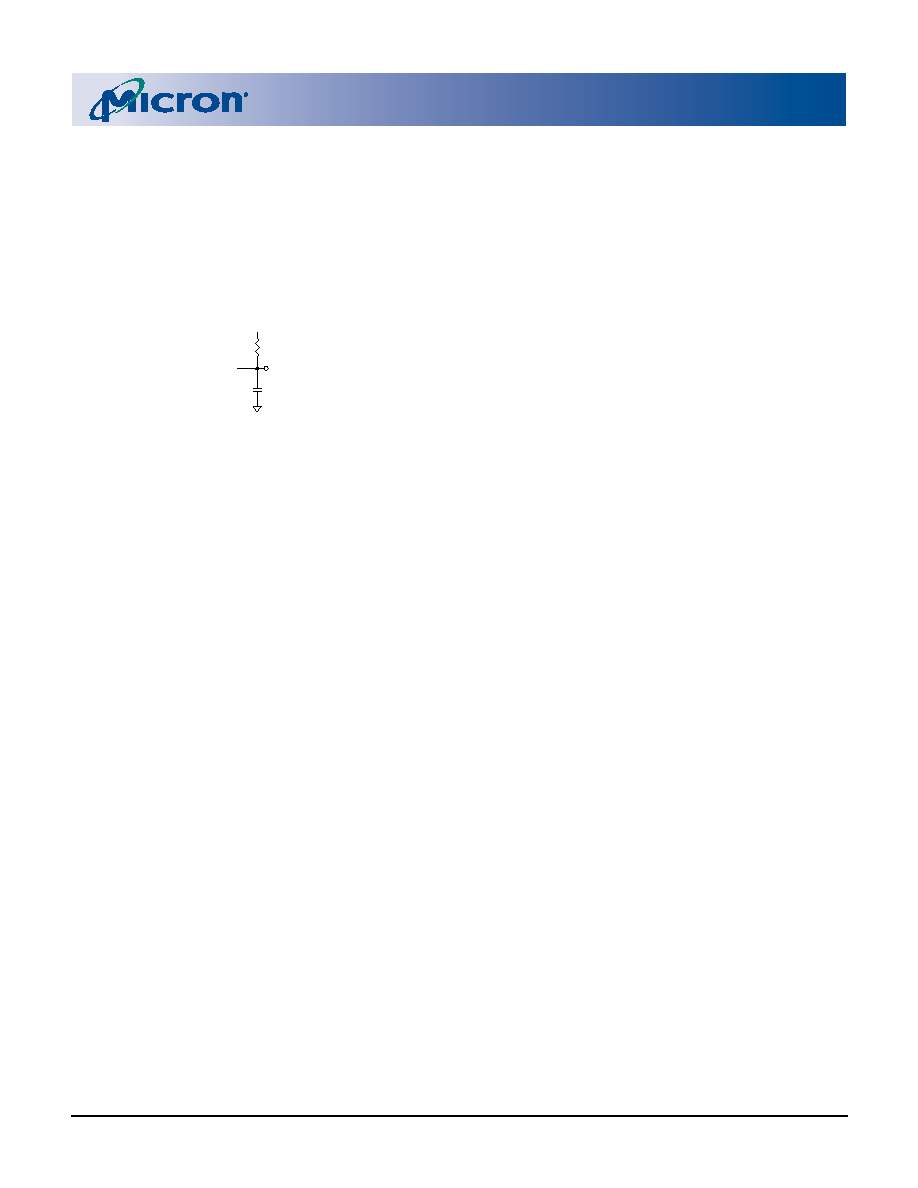
Output
(VOUT)
Reference
Point
50
VTT
30pF
相关PDF资料 |
PDF描述 |
|---|---|
| MT46V32M16BN-5BLIT | 32M X 16 DDR DRAM, 0.7 ns, PBGA60 |
| MT46V32M81AZ4-6T:G | 32M X 4 DDR DRAM, 0.75 ns, PDSO66 |
| MT47H128M8HV-187ELIT:E | 128M X 8 DDR DRAM, 0.35 ns, PBGA60 |
| MT47H128M8HQ-187ELAT:E | 128M X 8 DDR DRAM, 0.35 ns, PBGA60 |
| MT48LC2M32B1TG-7 | 2M X 32 SYNCHRONOUS DRAM, 5.5 ns, PDSO86 |
相关代理商/技术参数 |
参数描述 |
|---|---|
| MT46V32M16TG-75L | 制造商:MICRON 制造商全称:Micron Technology 功能描述:DOUBLE DATA RATE DDR SDRAM |
| MT46V32M16TG-75Z | 制造商:MICRON 制造商全称:Micron Technology 功能描述:DOUBLE DATA RATE DDR SDRAM |
| MT46V32M16TG-75ZL | 制造商:MICRON 制造商全称:Micron Technology 功能描述:DOUBLE DATA RATE DDR SDRAM |
发布紧急采购,3分钟左右您将得到回复。