- 您现在的位置:买卖IC网 > PDF目录224506 > MT46V32M81AZ4-6T:G 32M X 4 DDR DRAM, 0.75 ns, PDSO66 PDF资料下载
参数资料
| 型号: | MT46V32M81AZ4-6T:G |
| 元件分类: | DRAM |
| 英文描述: | 32M X 4 DDR DRAM, 0.75 ns, PDSO66 |
| 封装: | 0.400 INCH, PLASTIC, TSOP-66 |
| 文件页数: | 5/82页 |
| 文件大小: | 2866K |
第1页第2页第3页第4页当前第5页第6页第7页第8页第9页第10页第11页第12页第13页第14页第15页第16页第17页第18页第19页第20页第21页第22页第23页第24页第25页第26页第27页第28页第29页第30页第31页第32页第33页第34页第35页第36页第37页第38页第39页第40页第41页第42页第43页第44页第45页第46页第47页第48页第49页第50页第51页第52页第53页第54页第55页第56页第57页第58页第59页第60页第61页第62页第63页第64页第65页第66页第67页第68页第69页第70页第71页第72页第73页第74页第75页第76页第77页第78页第79页第80页第81页第82页
128Mb: x4, x8, x16
DDR SDRAM
09005aef8074a655
Micron Technology, Inc., reserves the right to change products or specifications without notice.
128MBDDRx4x8x16_2.fm - Rev. J 7/04 EN
13
2000 Micron Technology, Inc. All rights reserved.
Burst Length
Read and write accesses to the DDR SDRAM are
burst oriented, with the burst length being program-
mable, as shown in Figure 7. The burst length deter-
mines the maximum number of column locations that
can be accessed for a given READ or WRITE command.
Burst lengths of 2, 4, or 8 locations are available for
both the sequential and the interleaved burst types.
Reserved states should not be used, as unknown
operation or incompatibility with future versions may
result.
When a READ or WRITE command is issued, a block
of columns equal to the burst length is effectively
selected. All accesses for that burst take place within
this block, meaning that the burst will wrap within the
block if a boundary is reached. The block is uniquely
selected by A1-Ai when the burst length is set to two,
by A2-Ai when the burst length is set to four and by A3-
Ai when the burst length is set to eight (where Ai is the
most significant column address bit for a given config-
uration). The remaining (least significant) address
bit(s) is (are) used to select the starting location within
the block. The programmed burst length applies to
both READ and WRITE bursts.
Burst Type
Accesses within a given burst may be programmed
to be either sequential or interleaved; this is referred to
as the burst type and is selected via bit M3.
The ordering of accesses within a burst is deter-
mined by the burst length, the burst type and the start-
ing column address, as shown in Table 4, Burst
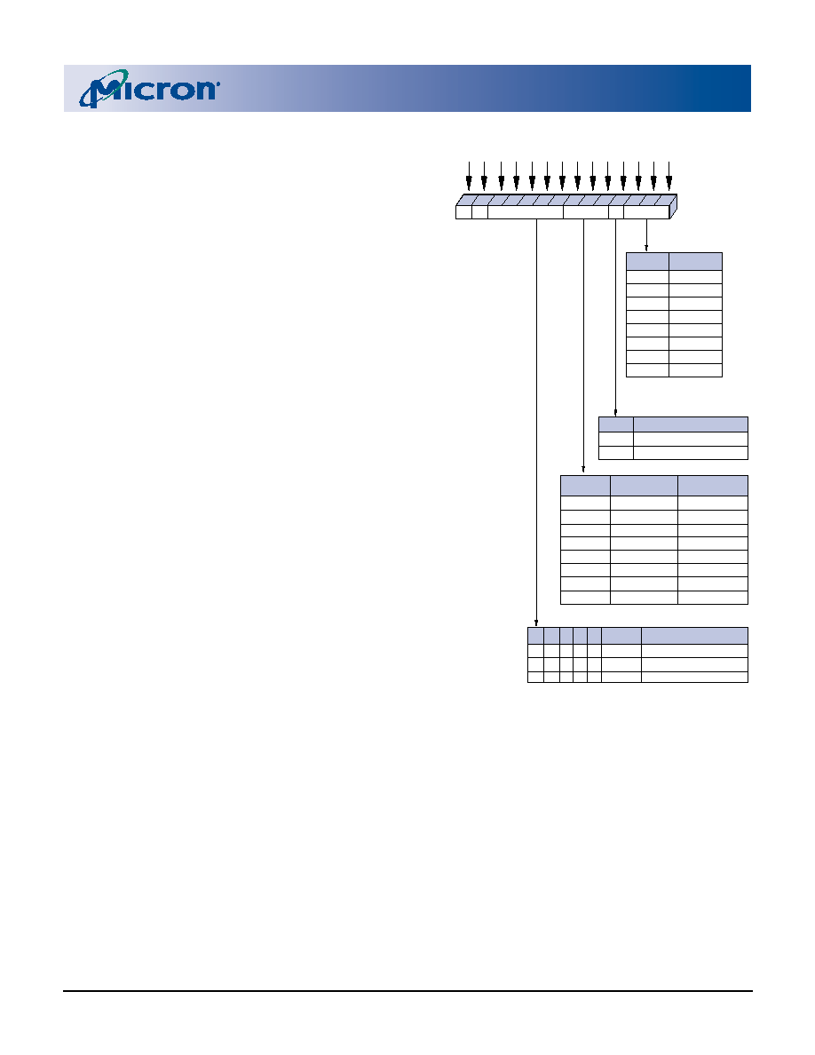
Figure 7: Mode Register Definition
Operating Mode
Normal Operation
Normal Operation/Reset DLL
All other states reserved
0
1
-
0
-
0
-
0
-
0
-
Valid
-
0
1
Burst Type
Sequential
Interleaved
CAS Latency
Reserved
2
Reserved
2.5
Reserved
Burst Length
CAS Latency BT
0*
A9
A7 A6 A5 A4 A3
A8
A2 A1 A0
Mode Register (Mx)
Address Bus
9
7
65
4
3
8
2
1
0
M3
M4
0
1
0
1
0
1
0
1
M5
0
1
0
1
M6
0
1
M6-M0
M8 M7
Operating Mode
A10
A11
BA0
BA1
10
11
12
0*
13
* M13 and M12 (BA1 and BA0)
must be “0, 0” to select the
base mode register (vs. the
extended mode register).
M9
M10
M11
Burst Length
Reserved
2
4
8
Reserved
M0
0
1
0
1
0
1
0
1
M1
0
1
0
1
M2
0
1
DDR400
CAS Latency
Reserved
2
3
Reserved
2.5
Reserved
相关PDF资料 |
PDF描述 |
|---|---|
| MT47H128M8HV-187ELIT:E | 128M X 8 DDR DRAM, 0.35 ns, PBGA60 |
| MT47H128M8HQ-187ELAT:E | 128M X 8 DDR DRAM, 0.35 ns, PBGA60 |
| MT48LC2M32B1TG-7 | 2M X 32 SYNCHRONOUS DRAM, 5.5 ns, PDSO86 |
| MT48LC32M4A2P-7ELIT:G | 32M X 4 SYNCHRONOUS DRAM, 5.4 ns, PDSO54 |
| MT55L256L18FT-12TR | 256K X 18 ZBT SRAM, 9 ns, PQFP100 |
相关代理商/技术参数 |
参数描述 |
|---|---|
| MT46V32M82ZZ5-75 ES | 制造商:Micron Technology Inc 功能描述:32MX8 SDRAM DDR PLASTIC PBF FBGA 2.5V - Trays |
| MT46V32M82ZZ5-75EZ | 制造商:Micron Technology Inc 功能描述:32MX8 DDR SDRAM PLASTIC 2.5V - Trays |
发布紧急采购,3分钟左右您将得到回复。