- 您现在的位置:买卖IC网 > PDF目录385639 > MT46V64M4 (Micron Technology, Inc.) 16 Meg x 4 x 4 banks DDR SDRAM(16M x 4 x 4组,双数据速率同步动态RAM) PDF资料下载
参数资料
| 型号: | MT46V64M4 |
| 厂商: | Micron Technology, Inc. |
| 英文描述: | 16 Meg x 4 x 4 banks DDR SDRAM(16M x 4 x 4组,双数据速率同步动态RAM) |
| 中文描述: | 16梅格× 4 × 4银行DDR SDRAM内存(1,600 × 4 × 4组,双数据速率同步动态RAM)的 |
| 文件页数: | 26/69页 |
| 文件大小: | 2410K |
| 代理商: | MT46V64M4 |
第1页第2页第3页第4页第5页第6页第7页第8页第9页第10页第11页第12页第13页第14页第15页第16页第17页第18页第19页第20页第21页第22页第23页第24页第25页当前第26页第27页第28页第29页第30页第31页第32页第33页第34页第35页第36页第37页第38页第39页第40页第41页第42页第43页第44页第45页第46页第47页第48页第49页第50页第51页第52页第53页第54页第55页第56页第57页第58页第59页第60页第61页第62页第63页第64页第65页第66页第67页第68页第69页
26
256Mb: x4, x8, x16 DDR SDRAM
256Mx4x8x16DDR_B.p65
–
Rev. B; Pub. 7/00
Micron Technology, Inc., reserves the right to change products or specifications without notice.
2000, Micron Technology, Inc.
256Mb: x4, x8, x16
DDR SDRAM
ADVANCE
WRITEs
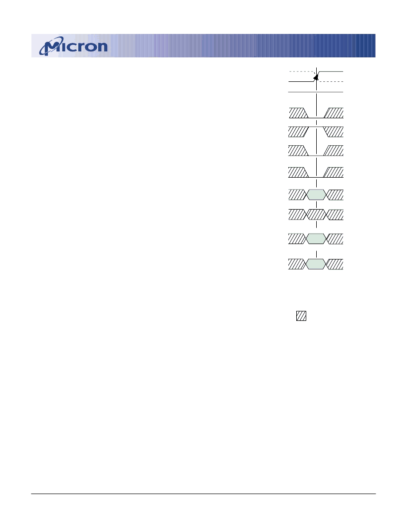
WRITE bursts are initiated with a WRITE command,
as shown in Figure 14.
The starting column and bank addresses are provided
with the WRITE command, and auto precharge is either
enabled or disabled for that access. If auto precharge is
enabled, the row being accessed is precharged at the
completion of the burst. For the generic WRITE com-
mands used in the following illustrations, auto precharge
is disabled.
During WRITE bursts, the first valid data-in element
will be registered on the first rising edge of DQS follow-
ing the WRITE command, and subsequent data ele-
ments will be registered on successive edges of DQS. The
LOW state on DQS between the WRITE command and
the first rising edge is known as the write preamble; the
LOW state on DQS following the last data-in element is
known as the write postamble.
The time between the WRITE command and the first
corresponding rising edge of DQS (
t
DQSS) is specified
with a relatively wide range (from 75 percent to 125
percent of one clock cycle). All of the WRITE diagrams
show the nominal case, and where the two extreme cases
(i.e.,
t
DQSS [MIN] and
t
DQSS
[MAX]) might not be
intuitive, they have also been included. Figure 15 shows
the nominal case and the extremes of
t
DQSS for a burst
of 4. Upon completion of a burst, assuming no other
commands have been initiated, the DQs will remain
High-Z and any additional input data will be ignored.
Data for any WRITE burst may be concatenated with
or truncated with a subsequent WRITE command. In
either case, a continuous flow of input data can be
maintained. The new WRITE command can be issued on
any positive edge of clock following the previous WRITE
command. The first data element from the new burst is
applied after either the last element of a completed burst
or the last desired data element of a longer burst which
is being truncated. The new WRITE command should be
issued
x
cycles after the first WRITE command, where
x
equals the number of desired data element pairs (pairs
are required by the 2
n
-prefetch architecture).
Figure 16 shows concatenated bursts of 4. An ex-
ample of nonconsecutive WRITEs is shown in Figure 17.
Full-speed random write accesses within a page or pages
can be performed as shown in Figure 18.
Data for any WRITE burst may be followed by a
subsequent READ command. To follow a WRITE with-
out truncating the WRITE burst,
t
WTR should be met as
shown in Figure 19.
Data for any WRITE burst may be truncated by a
subsequent READ command, as shown in Figure 20.
Note that only the data-in pairs that are registered prior
to the
t
WTR period are written to the internal array, and
Figure 14
WRITE Command
any subsequent data-in should be masked with DM as
shown in Figure 21.
Data for any WRITE burst may be followed by a
subsequent PRECHARGE command. To follow a WRITE
without truncating the WRITE burst,
t
WR should be met
as shown in Figure 22.
Data for any WRITE burst may be truncated by a
subsequent PRECHARGE command, as shown in Figures
23 and 24. Note that only the data-in pairs that are
registered prior to the
t
WR period are written to the
internal array, and any subsequent data-in should be
masked with DM as shown in Figures 23 and 24. After the
PRECHARGE command, a subsequent command to the
same bank cannot be issued until
t
RP is met.
CS#
WE#
CAS#
RAS#
CKE
CA
A10
BA0,1
HIGH
EN AP
DIS AP
BA
CK
CK#
CA = Column Address
BA = Bank Address
EN AP = Enable Auto Precharge
DIS AP = Disable Auto Precharge
DON
’
T CARE
x4: A0
–
A9, A11
x8: A0
–
A9
x16: A0
–
A8
x4: A12
x8: A11, A12
x16: A9, A11, A12
相关PDF资料 |
PDF描述 |
|---|---|
| MT46V64M8 | 16 Meg x 8 x 4 banks DDR SDRAM(16M x 8 x 4组,双数据速率同步动态RAM) |
| MT48LC16M8A1TG | SYNCHRONOUS DRAM |
| MT48LC32M4A1 | ECONOLINE: RSZ/P - 1kVDC |
| MT48LC32M4A2 | SYNCHRONOUS DRAM |
| MT48LC32M4A1TG | SYNCHRONOUS DRAM |
相关代理商/技术参数 |
参数描述 |
|---|---|
| MT46V64M4_1 | 制造商:MICRON 制造商全称:Micron Technology 功能描述:Double Data Rate (DDR) SDRAM |
发布紧急采购,3分钟左右您将得到回复。