- 您现在的位置:买卖IC网 > PDF目录385639 > MT46V64M4 (Micron Technology, Inc.) 16 Meg x 4 x 4 banks DDR SDRAM(16M x 4 x 4组,双数据速率同步动态RAM) PDF资料下载
参数资料
| 型号: | MT46V64M4 |
| 厂商: | Micron Technology, Inc. |
| 英文描述: | 16 Meg x 4 x 4 banks DDR SDRAM(16M x 4 x 4组,双数据速率同步动态RAM) |
| 中文描述: | 16梅格× 4 × 4银行DDR SDRAM内存(1,600 × 4 × 4组,双数据速率同步动态RAM)的 |
| 文件页数: | 65/69页 |
| 文件大小: | 2410K |
| 代理商: | MT46V64M4 |
第1页第2页第3页第4页第5页第6页第7页第8页第9页第10页第11页第12页第13页第14页第15页第16页第17页第18页第19页第20页第21页第22页第23页第24页第25页第26页第27页第28页第29页第30页第31页第32页第33页第34页第35页第36页第37页第38页第39页第40页第41页第42页第43页第44页第45页第46页第47页第48页第49页第50页第51页第52页第53页第54页第55页第56页第57页第58页第59页第60页第61页第62页第63页第64页当前第65页第66页第67页第68页第69页
65
256Mb: x4, x8, x16 DDR SDRAM
256Mx4x8x16DDR_B.p65
–
Rev. B; Pub. 7/00
Micron Technology, Inc., reserves the right to change products or specifications without notice.
2000, Micron Technology, Inc.
256Mb: x4, x8, x16
DDR SDRAM
ADVANCE
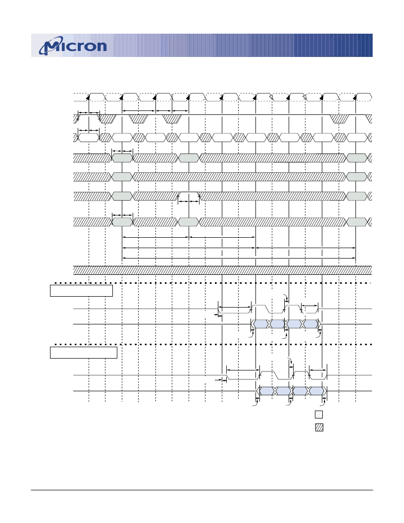
BANK READ – WITH AUTO PRECHARGE
CK
CK#
CKE
A10
BA0, BA1
t
CK
t
CH
t
CL
t
IS
t
IS
t
IH
t
IS
t
IS
t
IH
t
IH
t
IH
IS
IH
RA
t
RC
t
RP
CL = 2
DM
T0
T1
T2
T3
T4
T5
T5n
T6n
T6
T7
T8
DQ
1
DQS
Case 1:
t
AC
MIN
and
t
DQSCK
MIN
Case 2:
t
AC
(
MAX)
and
t
DQSCK
(
MAX)
DQ
1
DQS
t
RPRE
t
RPRE
t
RPST
t
RPST
t
DQSCK
(
MIN)
t
DQSCK
(
MAX)
t
AC
(
MIN)
t
LZ
(
MIN)
DO
n
t
HZ
(
MAX)
t
AC
(
MAX)
t
LZ
(
MAX)
DO
n
NOP5
NOP5
COMMAND
4
3
ACT
RA
RA
Col
n
READ2,6
NOP5
Bank
x
RA
RA
RA
Bank
x
ACT
Bank
x
NOP5
NOP5
NOP5
t
HZ
(
MIN)
NOTE:
1. DO
n
= data-out from column
n;
subsequent elements are provided in the programmed order.
2. Burst length = 4 in the case shown.
3. Enable auto precharge.
4. ACT = ACTIVE, RA = Row Address, BA = Bank Address.
5. NOP commands are shown for ease of illustration; other commands may be valid at these times.
6. The READ command can only be applied at T3 if
t
RAP is satisfied at T3
7. Refer to figure 27, 27A, and 28 for detailed DQS and DQ timing.
DON
’
T CARE
TRANSITIONING DATA
x4: A0-A9, A11
x8: A0-A9
x16: A0-A8
x4: A12
x8: A11, A12
x16: A9, A11, A12
t
RAS
t
LZ
(
MIN)
t
LZ
(
MAX)
t
RCD,
t
RAP6
相关PDF资料 |
PDF描述 |
|---|---|
| MT46V64M8 | 16 Meg x 8 x 4 banks DDR SDRAM(16M x 8 x 4组,双数据速率同步动态RAM) |
| MT48LC16M8A1TG | SYNCHRONOUS DRAM |
| MT48LC32M4A1 | ECONOLINE: RSZ/P - 1kVDC |
| MT48LC32M4A2 | SYNCHRONOUS DRAM |
| MT48LC32M4A1TG | SYNCHRONOUS DRAM |
相关代理商/技术参数 |
参数描述 |
|---|---|
| MT46V64M4_1 | 制造商:MICRON 制造商全称:Micron Technology 功能描述:Double Data Rate (DDR) SDRAM |
发布紧急采购,3分钟左右您将得到回复。