- 您现在的位置:买卖IC网 > PDF目录268181 > NAND01GW3B2AN6F (NUMONYX) 128M X 8 FLASH 3V PROM, 25000 ns, PDSO48 PDF资料下载
参数资料
| 型号: | NAND01GW3B2AN6F |
| 厂商: | NUMONYX |
| 元件分类: | PROM |
| 英文描述: | 128M X 8 FLASH 3V PROM, 25000 ns, PDSO48 |
| 封装: | 12 X 20 MM, LEAD FREE, PLASTIC, TSOP-48 |
| 文件页数: | 13/64页 |
| 文件大小: | 632K |
| 代理商: | NAND01GW3B2AN6F |
第1页第2页第3页第4页第5页第6页第7页第8页第9页第10页第11页第12页当前第13页第14页第15页第16页第17页第18页第19页第20页第21页第22页第23页第24页第25页第26页第27页第28页第29页第30页第31页第32页第33页第34页第35页第36页第37页第38页第39页第40页第41页第42页第43页第44页第45页第46页第47页第48页第49页第50页第51页第52页第53页第54页第55页第56页第57页第58页第59页第60页第61页第62页第63页第64页
Bus operations
NAND01G-B, NAND02G-B
20/64
4.4
Data Output
Data Output bus operations are used to read: the data in the memory array, the Status
Register, the lock status, the Electronic Signature and the Unique Identifier.
Data is output when Chip Enable is Low, Write Enable is High, Address Latch Enable is Low,
and Command Latch Enable is Low. The data is output sequentially using the Read Enable
signal.
4.5
Write Protect
Write Protect bus operations are used to protect the memory against program or erase
operations. When the Write Protect signal is Low the device will not accept program or erase
operations and so the contents of the memory array cannot be altered. The Write Protect
signal is not latched by Write Enable to ensure protection even during power-up.
4.6
Standby
When Chip Enable is High the memory enters Standby mode, the device is deselected,
outputs are disabled and power consumption is reduced.
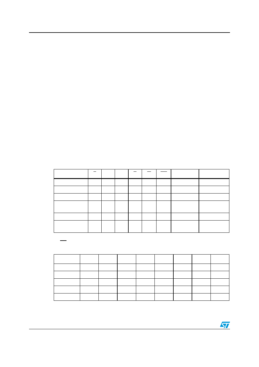
Table 5.
Bus Operations
Bus Operation
E
AL
CL
R
W
WP
I/O0 - I/O7
I/O8 - I/O15(1)
1. Only for x16 devices.
Command Input
VIL
VIH
Rising
X(2)
2. WP must be VIH when issuing a program or erase command.
Command
X
Address Input
VIL
VIH
VIL
VIH
Rising
X
Address
X
Data Input
VIL
VIH
Rising
VIH
Data Input
Data Output
VIL
Fallin
g
VIH
X
Data Output
Write Protect
X
VIL
XX
Standby
VIH
XX
X
VIL/VD
D
XX
Table 6.
Address Insertion, x8 Devices
Bus Cycle(1)
1.
Any additional address input cycles will be ignored.
I/O7
I/O6
I/O5
I/O4
I/O3
I/O2
I/O1
I/O0
1st
A7
A6
A5
A4
A3
A2
A1
A0
2nd
VIL
A11
A10
A9
A8
3rd
A19
A18
A17
A16
A15
A14
A13
A12
4th
A27
A26
A25
A24
A23
A22
A21
A20
5th(2)
2.
The fifth cycle is valid for 2Gb devices. A28 is for 2Gb devices only.
VIL
A28
相关PDF资料 |
PDF描述 |
|---|---|
| NAND08GW3B2CZC1 | 1G X 8 FLASH 3V PROM, 35 ns, PBGA63 |
| NAND01GR3B3CZA1 | 128M X 8 FLASH 1.8V PROM, 35 ns, PBGA63 |
| NAND02GR4B2BZB1 | 128M X 16 FLASH 1.8V PROM, 35 ns, PBGA63 |
| NCH030A3-FREQ-OUT27 | CRYSTAL OSCILLATOR, CLOCK, 1 MHz - 4 MHz, HCMOS OUTPUT |
| NTHA3JAA3-FREQ-OUT27 | CRYSTAL OSCILLATOR, CLOCK, 1 MHz - 4 MHz, HCMOS OUTPUT |
相关代理商/技术参数 |
参数描述 |
|---|---|
| NAND01GW3B2AN6T | 功能描述:闪存 NAND & S.MEDIA FLASH RoHS:否 制造商:ON Semiconductor 数据总线宽度:1 bit 存储类型:Flash 存储容量:2 MB 结构:256 K x 8 定时类型: 接口类型:SPI 访问时间: 电源电压-最大:3.6 V 电源电压-最小:2.3 V 最大工作电流:15 mA 工作温度:- 40 C to + 85 C 安装风格:SMD/SMT 封装 / 箱体: 封装:Reel |
| NAND01GW3B2AZA1 | 制造商:STMICROELECTRONICS 制造商全称:STMicroelectronics 功能描述:1 Gbit, 2 Gbit, 2112 Byte/1056 Word Page, 1.8V/3V, NAND Flash Memory |
| NAND01GW3B2AZA6 | 制造商:STMICROELECTRONICS 制造商全称:STMicroelectronics 功能描述:1 Gbit, 2 Gbit, 2112 Byte/1056 Word Page, 1.8V/3V, NAND Flash Memory |
| NAND01GW3B2AZA6E | 功能描述:闪存 NAND MEDIA FLASH RoHS:否 制造商:ON Semiconductor 数据总线宽度:1 bit 存储类型:Flash 存储容量:2 MB 结构:256 K x 8 定时类型: 接口类型:SPI 访问时间: 电源电压-最大:3.6 V 电源电压-最小:2.3 V 最大工作电流:15 mA 工作温度:- 40 C to + 85 C 安装风格:SMD/SMT 封装 / 箱体: 封装:Reel |
| NAND01GW3B2AZA6F | 制造商:Micron Technology Inc 功能描述:FLASH PARALLEL 3.3V 1GBIT 128MX8 25US 63VFBGA - Tape and Reel |
发布紧急采购,3分钟左右您将得到回复。