- 您现在的位置:买卖IC网 > PDF目录189449 > OR4E041BM680-DB (LATTICE SEMICONDUCTOR CORP) FPGA, 1296 CLBS, 380000 GATES, PBGA680 PDF资料下载
参数资料
| 型号: | OR4E041BM680-DB |
| 厂商: | LATTICE SEMICONDUCTOR CORP |
| 元件分类: | FPGA |
| 英文描述: | FPGA, 1296 CLBS, 380000 GATES, PBGA680 |
| 封装: | PLASTIC, FBGA-680 |
| 文件页数: | 108/151页 |
| 文件大小: | 2680K |
| 代理商: | OR4E041BM680-DB |
第1页第2页第3页第4页第5页第6页第7页第8页第9页第10页第11页第12页第13页第14页第15页第16页第17页第18页第19页第20页第21页第22页第23页第24页第25页第26页第27页第28页第29页第30页第31页第32页第33页第34页第35页第36页第37页第38页第39页第40页第41页第42页第43页第44页第45页第46页第47页第48页第49页第50页第51页第52页第53页第54页第55页第56页第57页第58页第59页第60页第61页第62页第63页第64页第65页第66页第67页第68页第69页第70页第71页第72页第73页第74页第75页第76页第77页第78页第79页第80页第81页第82页第83页第84页第85页第86页第87页第88页第89页第90页第91页第92页第93页第94页第95页第96页第97页第98页第99页第100页第101页第102页第103页第104页第105页第106页第107页当前第108页第109页第110页第111页第112页第113页第114页第115页第116页第117页第118页第119页第120页第121页第122页第123页第124页第125页第126页第127页第128页第129页第130页第131页第132页第133页第134页第135页第136页第137页第138页第139页第140页第141页第142页第143页第144页第145页第146页第147页第148页第149页第150页第151页
6
Lattice Semiconductor
Data Sheet
September, 2002
ORCA Series 4 FPGAs
Product Description (continued)
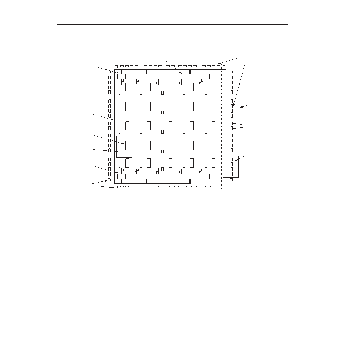
Note: For FPSCs, all I/Os and the four PLLs on the right side of the device are replaced with the embedded core.
5-7536(F)a
Figure 1. Series 4 Top Level Diagram
Programmable Logic Cells
The PLCs are arranged in an array of rows and columns. The location of a PLC is indicated by its row and column
so that a PLC in the second row and the third column is R2C3. The array of actual PLCs for every device begins
with R3C2 in all Series 4 generic FPGAs. PIOs are located on all four sides of the FPGA. Every group of four PIOs
on the device edge have an associated PIC.
The PLC consists of a PFU, SLIC, and routing resources. Each PFU within a PLC contains eight
4-input (16-bit) LUTs, eight latches/FFs, and one additional FF that may be used independently or with arithmetic
functions. The PFU is the main logic element of the PLC, containing elements for both combinatorial and sequential
logic. Combinatorial logic is done in LUTs located in the PFU. The PFU can be used in different modes to meet dif-
ferent logic requirements. The LUTs twin-quad architecture provides a congurable medium-/large-grain architec-
ture that can be used to implement from one to eight independent combinatorial logic functions or a large number
of complex logic functions using multiple LUTs. The exibility of the LUT to handle wide input functions, as well as
multiple smaller input functions, maximizes the gate count per PFU while increasing system speed.
The PFU is organized in a twin-quad fashion: two sets of four LUTs and FFs that can be controlled independently.
Each PFU has two independent programmable clocks, clock enables, local set/reset, and data selects.
LUTs may also be combined for use in arithmetic functions using fast-carry chain logic in either 4-bit or 8-bit
modes. The carry-out of either mode may be registered in the ninth FF for pipelining. Each PFU may also be con-
gured as a synchronous 32x4 single- or dual-port RAM or ROM. The FFs (or latches) may obtain input from LUT
outputs or directly from invertible PFU inputs, or they can be tied high or tied low. The FFs also have programmable
clock polarity, clock enables, and local set/reset.
EMBEDDED
SYSTEM BUS
PIC
PLC
MICROPROCESSOR
INTERFACE (MPI)
PFU
SLIC
FPGA/SYSTEM
BUS INTERFACE
PLLs
EMBEDDED
BLOCK RAM
HIGH-SPEED I/Os
CLOCK PINS
PIO
REPLACED BY
EMBEDDED IP
CORE FOR FPSCs
(ALL 4 SIDES)
(ALL 4
CORNERS)
相关PDF资料 |
PDF描述 |
|---|---|
| OR4E042BA352-DB | FPGA, 1296 CLBS, 380000 GATES, PBGA352 |
| OR4E042BM416-DB | FPGA, 1296 CLBS, 380000 GATES, PBGA416 |
| OR4E042BM680-DB | FPGA, 1296 CLBS, 380000 GATES, PBGA680 |
| OR4E043BA352-DB | FPGA, 1296 CLBS, 380000 GATES, PBGA352 |
| OR4E043BM416-DB | FPGA, 1296 CLBS, 380000 GATES, PBGA416 |
相关代理商/技术参数 |
参数描述 |
|---|---|
| OR4E04-1BM680I | 功能描述:FPGA - 现场可编程门阵列 10368 LUT 466 I/O RoHS:否 制造商:Altera Corporation 系列:Cyclone V E 栅极数量: 逻辑块数量:943 内嵌式块RAM - EBR:1956 kbit 输入/输出端数量:128 最大工作频率:800 MHz 工作电源电压:1.1 V 最大工作温度:+ 70 C 安装风格:SMD/SMT 封装 / 箱体:FBGA-256 |
| OR4E04-2BA352C | 功能描述:FPGA - 现场可编程门阵列 10368 LUT 466 I/O RoHS:否 制造商:Altera Corporation 系列:Cyclone V E 栅极数量: 逻辑块数量:943 内嵌式块RAM - EBR:1956 kbit 输入/输出端数量:128 最大工作频率:800 MHz 工作电源电压:1.1 V 最大工作温度:+ 70 C 安装风格:SMD/SMT 封装 / 箱体:FBGA-256 |
| OR4E04-2BA352I | 功能描述:FPGA - 现场可编程门阵列 10368 LUT 466 I/O RoHS:否 制造商:Altera Corporation 系列:Cyclone V E 栅极数量: 逻辑块数量:943 内嵌式块RAM - EBR:1956 kbit 输入/输出端数量:128 最大工作频率:800 MHz 工作电源电压:1.1 V 最大工作温度:+ 70 C 安装风格:SMD/SMT 封装 / 箱体:FBGA-256 |
| OR4E04-2BM416C | 功能描述:FPGA - 现场可编程门阵列 10368 LUT 466 I/O RoHS:否 制造商:Altera Corporation 系列:Cyclone V E 栅极数量: 逻辑块数量:943 内嵌式块RAM - EBR:1956 kbit 输入/输出端数量:128 最大工作频率:800 MHz 工作电源电压:1.1 V 最大工作温度:+ 70 C 安装风格:SMD/SMT 封装 / 箱体:FBGA-256 |
| OR4E04-2BM416I | 功能描述:FPGA - 现场可编程门阵列 10368 LUT 466 I/O RoHS:否 制造商:Altera Corporation 系列:Cyclone V E 栅极数量: 逻辑块数量:943 内嵌式块RAM - EBR:1956 kbit 输入/输出端数量:128 最大工作频率:800 MHz 工作电源电压:1.1 V 最大工作温度:+ 70 C 安装风格:SMD/SMT 封装 / 箱体:FBGA-256 |
发布紧急采购,3分钟左右您将得到回复。