- 您现在的位置:买卖IC网 > PDF目录189449 > OR4E041BM680-DB (LATTICE SEMICONDUCTOR CORP) FPGA, 1296 CLBS, 380000 GATES, PBGA680 PDF资料下载
参数资料
| 型号: | OR4E041BM680-DB |
| 厂商: | LATTICE SEMICONDUCTOR CORP |
| 元件分类: | FPGA |
| 英文描述: | FPGA, 1296 CLBS, 380000 GATES, PBGA680 |
| 封装: | PLASTIC, FBGA-680 |
| 文件页数: | 79/151页 |
| 文件大小: | 2680K |
| 代理商: | OR4E041BM680-DB |
第1页第2页第3页第4页第5页第6页第7页第8页第9页第10页第11页第12页第13页第14页第15页第16页第17页第18页第19页第20页第21页第22页第23页第24页第25页第26页第27页第28页第29页第30页第31页第32页第33页第34页第35页第36页第37页第38页第39页第40页第41页第42页第43页第44页第45页第46页第47页第48页第49页第50页第51页第52页第53页第54页第55页第56页第57页第58页第59页第60页第61页第62页第63页第64页第65页第66页第67页第68页第69页第70页第71页第72页第73页第74页第75页第76页第77页第78页当前第79页第80页第81页第82页第83页第84页第85页第86页第87页第88页第89页第90页第91页第92页第93页第94页第95页第96页第97页第98页第99页第100页第101页第102页第103页第104页第105页第106页第107页第108页第109页第110页第111页第112页第113页第114页第115页第116页第117页第118页第119页第120页第121页第122页第123页第124页第125页第126页第127页第128页第129页第130页第131页第132页第133页第134页第135页第136页第137页第138页第139页第140页第141页第142页第143页第144页第145页第146页第147页第148页第149页第150页第151页
Lattice Semiconductor
33
Data Sheet
September, 2002
ORCA Series 4 FPGAs
Programmable Input/Output Cells (continued)
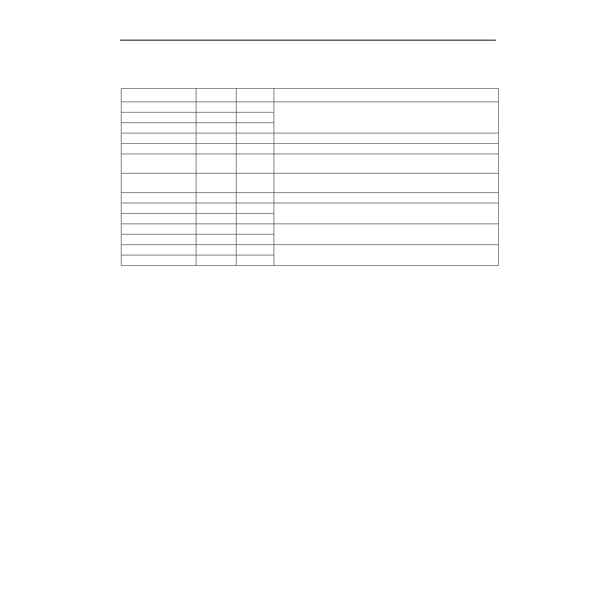
Table 13. Series 4 Programmable I/O Standards
Note: interfaces to DDR and ZBT memories are supported through the interface standards shown above.
The PIOs are located along the perimeter of the device. The PIO name is represented by a two-letter designation to
indicate the side of the device on which it is located followed by a number to indicate the row or column in which it is
located. The rst letter, P, designates that the cell is a PIO and not a PLC. The second letter indicates the side of the
array where the PIO is located. The four sides are left (L), right (R), top (T), and bottom (B). A number follows to
indicate the PIC row or column. The individual I/O pad is indicated by a single letter (either A, B, C, or D) placed at
the end of the PIO name. As an example, PL10A indicates a pad located on the left side of the array in the tenth
row.
Each PIC interfaces to four bond pads through four PIOs and contains the necessary routing resources to provide
an interface between I/O pads and the CIBs. Each PIC contains input buffers, output buffers, routing resources,
latches/FFs, and logic and can be congured as an input, output, or bidirectional I/O. Any PIO is capable of sup-
porting the I/O standards listed in Table 13.
The CIBs that connect to the PICs have signicant local routing resources, similar to routing in the PLCs. This new
routing increases the ability to x user pinouts prior to placement and routing of a design and still maintain routabil-
ity. The exibility provided by the routing also provides for increased signal speed due to a greater variety of optimal
signal paths.
Included in the routing interface is a fast path from the input pins to the PFU logic. This feature allows for input sig-
nals to be very quickly processed by the SLIC decoder function and used on-chip or sent back off of the FPGA.
A diagram of a single PIO is shown in Figure 22, and Table 14 provides an overview of the programmable functions
in an I/O cell.
Standard
VDDIO (V)
VREF (V)
Interface Usage
LVTTL
3.3
NA
General purpose.
LVCMOS2
2.5
NA
LVCMOS18
1.8
NA
PCI
3.3
NA
PCI.
LVDS
2.5
NA
Point to point and multi-drop backplanes, high noise immunity.
Bused-LVDS
2.5
NA
Network backplanes, high noise immunity, bus architecture
backplanes.
LVPECL
3.3
NA
Network backplanes, differential 100 MHz+ clocking, optical
transceiver, high-speed networking.
PECL
3.3
2.0
Backplanes.
GTL
3.3
0.8
Backplane or processor interface.
GTL+
3.3
1.0
HSTL-class I
1.5
0.75
High-speed SRAM and networking interfaces.
HTSL-class III and IV
1.5
0.9
STTL3-class I and II
3.3
1.5
Synchronous DRAM interface.
SSTL2-class I and II
2.5
1.25
相关PDF资料 |
PDF描述 |
|---|---|
| OR4E042BA352-DB | FPGA, 1296 CLBS, 380000 GATES, PBGA352 |
| OR4E042BM416-DB | FPGA, 1296 CLBS, 380000 GATES, PBGA416 |
| OR4E042BM680-DB | FPGA, 1296 CLBS, 380000 GATES, PBGA680 |
| OR4E043BA352-DB | FPGA, 1296 CLBS, 380000 GATES, PBGA352 |
| OR4E043BM416-DB | FPGA, 1296 CLBS, 380000 GATES, PBGA416 |
相关代理商/技术参数 |
参数描述 |
|---|---|
| OR4E04-1BM680I | 功能描述:FPGA - 现场可编程门阵列 10368 LUT 466 I/O RoHS:否 制造商:Altera Corporation 系列:Cyclone V E 栅极数量: 逻辑块数量:943 内嵌式块RAM - EBR:1956 kbit 输入/输出端数量:128 最大工作频率:800 MHz 工作电源电压:1.1 V 最大工作温度:+ 70 C 安装风格:SMD/SMT 封装 / 箱体:FBGA-256 |
| OR4E04-2BA352C | 功能描述:FPGA - 现场可编程门阵列 10368 LUT 466 I/O RoHS:否 制造商:Altera Corporation 系列:Cyclone V E 栅极数量: 逻辑块数量:943 内嵌式块RAM - EBR:1956 kbit 输入/输出端数量:128 最大工作频率:800 MHz 工作电源电压:1.1 V 最大工作温度:+ 70 C 安装风格:SMD/SMT 封装 / 箱体:FBGA-256 |
| OR4E04-2BA352I | 功能描述:FPGA - 现场可编程门阵列 10368 LUT 466 I/O RoHS:否 制造商:Altera Corporation 系列:Cyclone V E 栅极数量: 逻辑块数量:943 内嵌式块RAM - EBR:1956 kbit 输入/输出端数量:128 最大工作频率:800 MHz 工作电源电压:1.1 V 最大工作温度:+ 70 C 安装风格:SMD/SMT 封装 / 箱体:FBGA-256 |
| OR4E04-2BM416C | 功能描述:FPGA - 现场可编程门阵列 10368 LUT 466 I/O RoHS:否 制造商:Altera Corporation 系列:Cyclone V E 栅极数量: 逻辑块数量:943 内嵌式块RAM - EBR:1956 kbit 输入/输出端数量:128 最大工作频率:800 MHz 工作电源电压:1.1 V 最大工作温度:+ 70 C 安装风格:SMD/SMT 封装 / 箱体:FBGA-256 |
| OR4E04-2BM416I | 功能描述:FPGA - 现场可编程门阵列 10368 LUT 466 I/O RoHS:否 制造商:Altera Corporation 系列:Cyclone V E 栅极数量: 逻辑块数量:943 内嵌式块RAM - EBR:1956 kbit 输入/输出端数量:128 最大工作频率:800 MHz 工作电源电压:1.1 V 最大工作温度:+ 70 C 安装风格:SMD/SMT 封装 / 箱体:FBGA-256 |
发布紧急采购,3分钟左右您将得到回复。