- 您现在的位置:买卖IC网 > PDF目录189449 > OR4E041BM680-DB (LATTICE SEMICONDUCTOR CORP) FPGA, 1296 CLBS, 380000 GATES, PBGA680 PDF资料下载
参数资料
| 型号: | OR4E041BM680-DB |
| 厂商: | LATTICE SEMICONDUCTOR CORP |
| 元件分类: | FPGA |
| 英文描述: | FPGA, 1296 CLBS, 380000 GATES, PBGA680 |
| 封装: | PLASTIC, FBGA-680 |
| 文件页数: | 88/151页 |
| 文件大小: | 2680K |
| 代理商: | OR4E041BM680-DB |
第1页第2页第3页第4页第5页第6页第7页第8页第9页第10页第11页第12页第13页第14页第15页第16页第17页第18页第19页第20页第21页第22页第23页第24页第25页第26页第27页第28页第29页第30页第31页第32页第33页第34页第35页第36页第37页第38页第39页第40页第41页第42页第43页第44页第45页第46页第47页第48页第49页第50页第51页第52页第53页第54页第55页第56页第57页第58页第59页第60页第61页第62页第63页第64页第65页第66页第67页第68页第69页第70页第71页第72页第73页第74页第75页第76页第77页第78页第79页第80页第81页第82页第83页第84页第85页第86页第87页当前第88页第89页第90页第91页第92页第93页第94页第95页第96页第97页第98页第99页第100页第101页第102页第103页第104页第105页第106页第107页第108页第109页第110页第111页第112页第113页第114页第115页第116页第117页第118页第119页第120页第121页第122页第123页第124页第125页第126页第127页第128页第129页第130页第131页第132页第133页第134页第135页第136页第137页第138页第139页第140页第141页第142页第143页第144页第145页第146页第147页第148页第149页第150页第151页
Data Sheet
September, 2002
Lattice Semiconductor
41
ORCA Series 4 FPGAs
Special Function Blocks (continued)
5-6765(F)
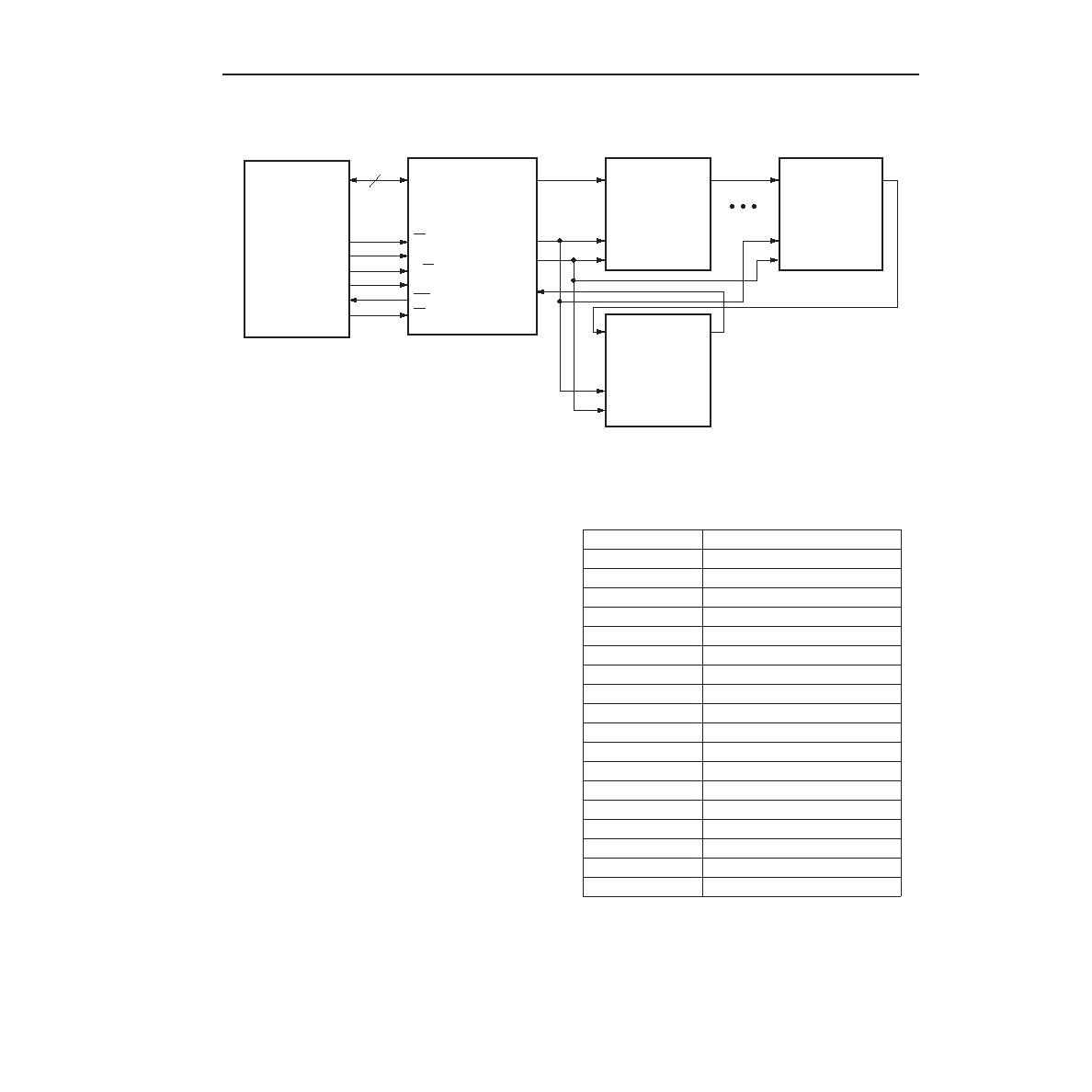
Figure 26. Boundary-Scan Interface
D[7:0]
INTR
MICRO-
PROCESSOR
D[7:0]
CE
RA
R/W
DAV
INT
SP
TMS0
TCK
TDI
TDO
TDI
TMS
TCK
TDO
ORCA
SERIES
FPGA
TDI
ORCA
SERIES
FPGA
TMS
TCK
TDO
TDI
TMS
TCK
TDO
ORCA
SERIES
FPGA
BOUNDARY-
SCAN
MASTER
(BSM)
(DUT)
The boundary-scan support circuit shown in Figure 26
is the 497AA boundary-scan master (BSM). The BSM
off-loads tasks from the test host to increase test
throughput. To interface between the test host and the
DUTs, the BSM has a general MPI and provides paral-
lel-to-serial/serial-to-parallel conversion, as well as
three 8K data buffers. The BSM also increases test
throughput with a dedicated automatic test-pattern
generator and with compression of the test response
with a signature analysis register. The PC-based
boundary-scan test card/software allows a user to
quickly prototype a boundary-scan test setup.
Boundary-Scan Instructions
The Series 4 boundary-scan circuitry supports a total
of 18 instructions. This includes ten IEEE 1149.1,
1149.2, and 1532/D1 instructions, one optional IEEE
1149.3 instruction, two IEEE 1532/D1 optional instruc-
tions, and ve ORCA-dened instructions. There are
also 16 other scan chain instructions that are used only
during factory device testing and will not be discussed
in this data sheet. A 6-bit wide instruction register sup-
ports all the instructions listed in Table 18.
The BYPASS instruction passes data intentionally from
TDI to TDO after being clocked by TCK.
Table 18. Boundary-Scan Instructions
Code
Instruction
000000
EXTEST
000001
SAMPLE
000011
PRELOAD
000100
RUNBIST
000101
IDCODE
000110
USERCODE
001000
ISC_ENABLE
001001
ISC_PROGRAM
001010
ISC_NOOP
001011
ISC_DISABLE
001101
ISC_PROGRAM_USERCODE
001110
ISC_READ
010001
PLC_SCAN_RING1
010010
PLC_SCAN_RING2
010011
PLC_SCAN_RING3
010100
RAM_WRITE
010101
RAM_READ
111111
BYPASS
相关PDF资料 |
PDF描述 |
|---|---|
| OR4E042BA352-DB | FPGA, 1296 CLBS, 380000 GATES, PBGA352 |
| OR4E042BM416-DB | FPGA, 1296 CLBS, 380000 GATES, PBGA416 |
| OR4E042BM680-DB | FPGA, 1296 CLBS, 380000 GATES, PBGA680 |
| OR4E043BA352-DB | FPGA, 1296 CLBS, 380000 GATES, PBGA352 |
| OR4E043BM416-DB | FPGA, 1296 CLBS, 380000 GATES, PBGA416 |
相关代理商/技术参数 |
参数描述 |
|---|---|
| OR4E04-1BM680I | 功能描述:FPGA - 现场可编程门阵列 10368 LUT 466 I/O RoHS:否 制造商:Altera Corporation 系列:Cyclone V E 栅极数量: 逻辑块数量:943 内嵌式块RAM - EBR:1956 kbit 输入/输出端数量:128 最大工作频率:800 MHz 工作电源电压:1.1 V 最大工作温度:+ 70 C 安装风格:SMD/SMT 封装 / 箱体:FBGA-256 |
| OR4E04-2BA352C | 功能描述:FPGA - 现场可编程门阵列 10368 LUT 466 I/O RoHS:否 制造商:Altera Corporation 系列:Cyclone V E 栅极数量: 逻辑块数量:943 内嵌式块RAM - EBR:1956 kbit 输入/输出端数量:128 最大工作频率:800 MHz 工作电源电压:1.1 V 最大工作温度:+ 70 C 安装风格:SMD/SMT 封装 / 箱体:FBGA-256 |
| OR4E04-2BA352I | 功能描述:FPGA - 现场可编程门阵列 10368 LUT 466 I/O RoHS:否 制造商:Altera Corporation 系列:Cyclone V E 栅极数量: 逻辑块数量:943 内嵌式块RAM - EBR:1956 kbit 输入/输出端数量:128 最大工作频率:800 MHz 工作电源电压:1.1 V 最大工作温度:+ 70 C 安装风格:SMD/SMT 封装 / 箱体:FBGA-256 |
| OR4E04-2BM416C | 功能描述:FPGA - 现场可编程门阵列 10368 LUT 466 I/O RoHS:否 制造商:Altera Corporation 系列:Cyclone V E 栅极数量: 逻辑块数量:943 内嵌式块RAM - EBR:1956 kbit 输入/输出端数量:128 最大工作频率:800 MHz 工作电源电压:1.1 V 最大工作温度:+ 70 C 安装风格:SMD/SMT 封装 / 箱体:FBGA-256 |
| OR4E04-2BM416I | 功能描述:FPGA - 现场可编程门阵列 10368 LUT 466 I/O RoHS:否 制造商:Altera Corporation 系列:Cyclone V E 栅极数量: 逻辑块数量:943 内嵌式块RAM - EBR:1956 kbit 输入/输出端数量:128 最大工作频率:800 MHz 工作电源电压:1.1 V 最大工作温度:+ 70 C 安装风格:SMD/SMT 封装 / 箱体:FBGA-256 |
发布紧急采购,3分钟左右您将得到回复。