- 您现在的位置:买卖IC网 > PDF目录189449 > OR4E041BM680-DB (LATTICE SEMICONDUCTOR CORP) FPGA, 1296 CLBS, 380000 GATES, PBGA680 PDF资料下载
参数资料
| 型号: | OR4E041BM680-DB |
| 厂商: | LATTICE SEMICONDUCTOR CORP |
| 元件分类: | FPGA |
| 英文描述: | FPGA, 1296 CLBS, 380000 GATES, PBGA680 |
| 封装: | PLASTIC, FBGA-680 |
| 文件页数: | 70/151页 |
| 文件大小: | 2680K |
| 代理商: | OR4E041BM680-DB |
第1页第2页第3页第4页第5页第6页第7页第8页第9页第10页第11页第12页第13页第14页第15页第16页第17页第18页第19页第20页第21页第22页第23页第24页第25页第26页第27页第28页第29页第30页第31页第32页第33页第34页第35页第36页第37页第38页第39页第40页第41页第42页第43页第44页第45页第46页第47页第48页第49页第50页第51页第52页第53页第54页第55页第56页第57页第58页第59页第60页第61页第62页第63页第64页第65页第66页第67页第68页第69页当前第70页第71页第72页第73页第74页第75页第76页第77页第78页第79页第80页第81页第82页第83页第84页第85页第86页第87页第88页第89页第90页第91页第92页第93页第94页第95页第96页第97页第98页第99页第100页第101页第102页第103页第104页第105页第106页第107页第108页第109页第110页第111页第112页第113页第114页第115页第116页第117页第118页第119页第120页第121页第122页第123页第124页第125页第126页第127页第128页第129页第130页第131页第132页第133页第134页第135页第136页第137页第138页第139页第140页第141页第142页第143页第144页第145页第146页第147页第148页第149页第150页第151页
Lattice Semiconductor
25
Data Sheet
September, 2002
ORCA Series 4 FPGAs
Programmable Logic Cells (continued)
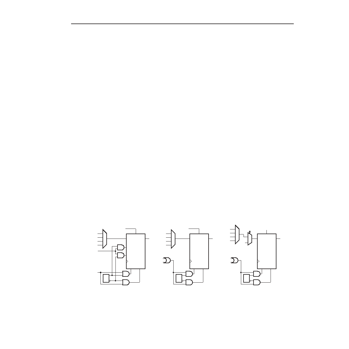
The set/reset operation of the latch/FF is controlled by
two parameters: reset mode and set/reset value. When
the GSRN and local set/reset (LSR) signals are not
asserted, the latch/FF operates normally. The reset
mode is used to select a synchronous or asynchronous
LSR operation. If synchronous, LSR has the option to
be enabled only if clock enable (CE) is active or for LSR
to have priority over the clock enable input, thereby set-
ting/resetting the FF independent of the state of the
clock enable. The clock enable is supported on FFs, not
latches. It is implemented by using a 2-input multiplexer
on the FF input, with one input being the previous state
of the FF and the other input being the new data
applied to the FF. The select of this 2-input multiplexer
is clock enable (CE), which selects either the new data
or the previous state. When the clock enable is inactive,
the FF output does not change when the clock edge
arrives.
The GSRN signal is only asynchronous, and it sets/
resets all latches/FFs in the FPGA based upon the set/
reset conguration bit for each latch/FF. The set/reset
value determines whether GSRN and LSR are set or
reset inputs. The set/reset value is independent for
each latch/FF. An option is available to disable the
GSRN function per PFU after initial device congura-
tion.
The latch/FF can be congured to have a data front-
end select. Two data inputs are possible in the front-end
select mode, with the SEL signal used to select which
data input is used. The data input into each
latch/FF is from the output of its associated LUT,
F[7:0], or direct from DIN[7:0], bypassing the LUT. In
the front-end data select mode, both signals are avail-
able to the latches/FFs.
If either or both of these inputs is unused or is unavail-
able, the latch/FF data input can be tied to a logic 0 or
logic 1 instead (the default is logic 0).
The latches/FFs can be congured in three basic
modes:
■
Local synchronous set/reset: the input into the PFU’s
LSR port is used to synchronously set or reset each
latch/FF.
■
Local asynchronous set/reset: the input into LSR
asynchronously sets or resets each latch/FF.
■
Latch/FF with front-end select, LSR either synchro-
nous or asynchronous: the data select signal selects
the input into the latches/FFs between the LUT out-
put and direct data in.
For all three modes, each latch/FF can be indepen-
dently programmed as either set or reset. Figure 20
provides the logic functionality of the front-end select,
global set/reset, and local set/reset operations.
The ninth PFU FF, which is generally associated with
registering the carry-out signal in ripple mode func-
tions, can be used as a general-purpose FF. It is only
an FF and is not capable of being congured as a
latch. Because the ninth FF is not associated with an
LUT, there is no front-end data select. The data input to
the ninth FF is limited to the CIN input, logic 1, logic 0,
or the carry-out in ripple and half-logic modes.
5-9737(F).a
Key: C = conguration data.
Figure 20. Latch/FF Set/Reset Congurations
CE
DQ
S_SET
S_RESET
CLK
SET RESET
F
DIN
LOGIC 1
LOGIC 0
LSR
CD
GSRN
CE
DQ
CLK
SET RESET
F
DIN
LOGIC 1
LOGIC 0
CD
GSRN
LSR
CE
DQ
CLK
SET RESET
F
DIN
LOGIC 1
LOGIC 0
CD
GSRN
LSR
DIN
SEL
相关PDF资料 |
PDF描述 |
|---|---|
| OR4E042BA352-DB | FPGA, 1296 CLBS, 380000 GATES, PBGA352 |
| OR4E042BM416-DB | FPGA, 1296 CLBS, 380000 GATES, PBGA416 |
| OR4E042BM680-DB | FPGA, 1296 CLBS, 380000 GATES, PBGA680 |
| OR4E043BA352-DB | FPGA, 1296 CLBS, 380000 GATES, PBGA352 |
| OR4E043BM416-DB | FPGA, 1296 CLBS, 380000 GATES, PBGA416 |
相关代理商/技术参数 |
参数描述 |
|---|---|
| OR4E04-1BM680I | 功能描述:FPGA - 现场可编程门阵列 10368 LUT 466 I/O RoHS:否 制造商:Altera Corporation 系列:Cyclone V E 栅极数量: 逻辑块数量:943 内嵌式块RAM - EBR:1956 kbit 输入/输出端数量:128 最大工作频率:800 MHz 工作电源电压:1.1 V 最大工作温度:+ 70 C 安装风格:SMD/SMT 封装 / 箱体:FBGA-256 |
| OR4E04-2BA352C | 功能描述:FPGA - 现场可编程门阵列 10368 LUT 466 I/O RoHS:否 制造商:Altera Corporation 系列:Cyclone V E 栅极数量: 逻辑块数量:943 内嵌式块RAM - EBR:1956 kbit 输入/输出端数量:128 最大工作频率:800 MHz 工作电源电压:1.1 V 最大工作温度:+ 70 C 安装风格:SMD/SMT 封装 / 箱体:FBGA-256 |
| OR4E04-2BA352I | 功能描述:FPGA - 现场可编程门阵列 10368 LUT 466 I/O RoHS:否 制造商:Altera Corporation 系列:Cyclone V E 栅极数量: 逻辑块数量:943 内嵌式块RAM - EBR:1956 kbit 输入/输出端数量:128 最大工作频率:800 MHz 工作电源电压:1.1 V 最大工作温度:+ 70 C 安装风格:SMD/SMT 封装 / 箱体:FBGA-256 |
| OR4E04-2BM416C | 功能描述:FPGA - 现场可编程门阵列 10368 LUT 466 I/O RoHS:否 制造商:Altera Corporation 系列:Cyclone V E 栅极数量: 逻辑块数量:943 内嵌式块RAM - EBR:1956 kbit 输入/输出端数量:128 最大工作频率:800 MHz 工作电源电压:1.1 V 最大工作温度:+ 70 C 安装风格:SMD/SMT 封装 / 箱体:FBGA-256 |
| OR4E04-2BM416I | 功能描述:FPGA - 现场可编程门阵列 10368 LUT 466 I/O RoHS:否 制造商:Altera Corporation 系列:Cyclone V E 栅极数量: 逻辑块数量:943 内嵌式块RAM - EBR:1956 kbit 输入/输出端数量:128 最大工作频率:800 MHz 工作电源电压:1.1 V 最大工作温度:+ 70 C 安装风格:SMD/SMT 封装 / 箱体:FBGA-256 |
发布紧急采购,3分钟左右您将得到回复。