- 您现在的位置:买卖IC网 > PDF目录225141 > S29WS064N0PBAW011 (Spansion Inc.) 256/128/64 MEGABIT CMOS 1.8 VOLT ONLY SIMULTANEOUS READ/WRITE BURST MODE FLASH MEMORY PDF资料下载
参数资料
| 型号: | S29WS064N0PBAW011 |
| 厂商: | Spansion Inc. |
| 英文描述: | 256/128/64 MEGABIT CMOS 1.8 VOLT ONLY SIMULTANEOUS READ/WRITE BURST MODE FLASH MEMORY |
| 中文描述: | 256/128/64兆位的CMOS 1.8伏只有同时读/写突发模式闪存 |
| 文件页数: | 26/99页 |
| 文件大小: | 1091K |
| 代理商: | S29WS064N0PBAW011 |
第1页第2页第3页第4页第5页第6页第7页第8页第9页第10页第11页第12页第13页第14页第15页第16页第17页第18页第19页第20页第21页第22页第23页第24页第25页当前第26页第27页第28页第29页第30页第31页第32页第33页第34页第35页第36页第37页第38页第39页第40页第41页第42页第43页第44页第45页第46页第47页第48页第49页第50页第51页第52页第53页第54页第55页第56页第57页第58页第59页第60页第61页第62页第63页第64页第65页第66页第67页第68页第69页第70页第71页第72页第73页第74页第75页第76页第77页第78页第79页第80页第81页第82页第83页第84页第85页第86页第87页第88页第89页第90页第91页第92页第93页第94页第95页第96页第97页第98页第99页
30
S29WS-N_00_G0 January 25, 2005
Adva nce
Information
Note: Base = Base Address.
The following is a C source code example of using the single word program function. Refer to
the Spansion Low Level Driver User’s Guide (available on www.amd.com and
www.fujitsu.com) for general information on Spansion Flash memory software development
guidelines.
/* Example: Program Command
*/
*( (UINT16 *)base_addr + 0x555 ) = 0x00AA;
/* write unlock cycle 1
*/
*( (UINT16 *)base_addr + 0x2AA ) = 0x0055;
/* write unlock cycle 2
*/
*( (UINT16 *)base_addr + 0x555 ) = 0x00A0;
/* write program setup command
*/
*( (UINT16 *)pa )
= data;
/* write data to be programmed
*/
/* Poll for program completion */
7.5.2 Write Buffer Programming
Write Buffer Programming allows the system to write a maximum of 32 words in one program-
ming operation. This results in a faster effective word programming time than the standard
“word” programming algorithms. The Write Buffer Programming command sequence is initiated
by first writing two unlock cycles. This is followed by a third write cycle containing the Write Buffer
Load command written at the Sector Address in which programming occurs. At this point, the sys-
tem writes the number of “word locations minus 1” that are loaded into the page buffer at the
Sector Address in which programming occurs. This tells the device how many write buffer ad-
dresses are loaded with data and therefore when to expect the “Program Buffer to Flash” confirm
command. The number of locations to program cannot exceed the size of the write buffer or the
operation aborts. (Number loaded = the number of locations to program minus 1. For example,
if the system programs 6 address locations, then 05h should be written to the device.)
The system then writes the starting address/data combination. This starting address is the first
address/data pair to be programmed, and selects the “write-buffer-page” address. All subsequent
address/data pairs must fall within the elected-write-buffer-page.
The “write-buffer-page” is selected by using the addresses AMAX - A5.
The “write-buffer-page” addresses must be the same for all address/data pairs loaded into the
write buffer. (This means Write Buffer Programming cannot be performed across multiple “write-
buffer-pages.” This also means that Write Buffer Programming cannot be performed across mul-
tiple sectors. If the system attempts to load programming data outside of the selected “write-
buffer-page”, the operation ABORTs.)
After writing the Starting Address/Data pair, the system then writes the remaining address/data
pairs into the write buffer.
Note that if a Write Buffer address location is loaded multiple times, the “address/data pair”
counter is decremented for every data load operation. Also, the last data loaded at a location be-
fore the “Program Buffer to Flash” confirm command is programmed into the device. It is the
software's responsibility to comprehend ramifications of loading a write-buffer location more than
Software Functions and Sample Code
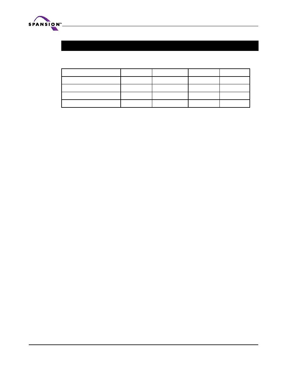
Table 7.12. Single Word Program
(LLD Function = lld_ProgramCmd)
Cycle
Operation
Byte Address
Word Address
Data
Unlock Cycle 1
Write
Base + AAAh
Base + 555h
00AAh
Unlock Cycle 2
Write
Base + 554h
Base + 2AAh
0055h
Program Setup
Write
Base + AAAh
Base + 555h
00A0h
Program
Write
Word Address
Data Word
相关PDF资料 |
PDF描述 |
|---|---|
| S29WS128N0LBFI111 | 256/128/64 MEGABIT CMOS 1.8 VOLT ONLY SIMULTANEOUS READ/WRITE BURST MODE FLASH MEMORY |
| S29WS128N0LBFI112 | 256/128/64 MEGABIT CMOS 1.8 VOLT ONLY SIMULTANEOUS READ/WRITE BURST MODE FLASH MEMORY |
| S29WS128N0LBFI113 | 256/128/64 MEGABIT CMOS 1.8 VOLT ONLY SIMULTANEOUS READ/WRITE BURST MODE FLASH MEMORY |
| S29WS128N0LBFW011 | Test Clip; Current Rating:100A; Body Material:Steel; Features:Unmarked; Jaw Opening Max:1.625"; Overall Length:6" RoHS Compliant: NA |
| S29WS128N0LBFI011 | 256/128/64 MEGABIT CMOS 1.8 VOLT ONLY SIMULTANEOUS READ/WRITE BURST MODE FLASH MEMORY |
相关代理商/技术参数 |
参数描述 |
|---|---|
| S29WS064N0PBAW012 | 制造商:SPANSION 制造商全称:SPANSION 功能描述:256/128/64 Megabit (16/8/4 M x 16-Bit) CMOS 1.8 Volt-only Simultaneous Read/Write, Burst Mode Flash Memory |
| S29WS064N0PBAW013 | 制造商:SPANSION 制造商全称:SPANSION 功能描述:256/128/64 MEGABIT CMOS 1.8 VOLT ONLY SIMULTANEOUS READ/WRITE BURST MODE FLASH MEMORY |
| S29WS064N0PBAW110 | 制造商:SPANSION 制造商全称:SPANSION 功能描述:256/128/64 MEGABIT CMOS 1.8 VOLT ONLY SIMULTANEOUS READ/WRITE BURST MODE FLASH MEMORY |
| S29WS064N0PBAW111 | 制造商:SPANSION 制造商全称:SPANSION 功能描述:256/128/64 MEGABIT CMOS 1.8 VOLT ONLY SIMULTANEOUS READ/WRITE BURST MODE FLASH MEMORY |
| S29WS064N0PBAW112 | 制造商:SPANSION 制造商全称:SPANSION 功能描述:256/128/64 MEGABIT CMOS 1.8 VOLT ONLY SIMULTANEOUS READ/WRITE BURST MODE FLASH MEMORY |
发布紧急采购,3分钟左右您将得到回复。