- 您现在的位置:买卖IC网 > PDF目录225141 > S29WS064N0PBAW011 (Spansion Inc.) 256/128/64 MEGABIT CMOS 1.8 VOLT ONLY SIMULTANEOUS READ/WRITE BURST MODE FLASH MEMORY PDF资料下载
参数资料
| 型号: | S29WS064N0PBAW011 |
| 厂商: | Spansion Inc. |
| 英文描述: | 256/128/64 MEGABIT CMOS 1.8 VOLT ONLY SIMULTANEOUS READ/WRITE BURST MODE FLASH MEMORY |
| 中文描述: | 256/128/64兆位的CMOS 1.8伏只有同时读/写突发模式闪存 |
| 文件页数: | 33/99页 |
| 文件大小: | 1091K |
| 代理商: | S29WS064N0PBAW011 |
第1页第2页第3页第4页第5页第6页第7页第8页第9页第10页第11页第12页第13页第14页第15页第16页第17页第18页第19页第20页第21页第22页第23页第24页第25页第26页第27页第28页第29页第30页第31页第32页当前第33页第34页第35页第36页第37页第38页第39页第40页第41页第42页第43页第44页第45页第46页第47页第48页第49页第50页第51页第52页第53页第54页第55页第56页第57页第58页第59页第60页第61页第62页第63页第64页第65页第66页第67页第68页第69页第70页第71页第72页第73页第74页第75页第76页第77页第78页第79页第80页第81页第82页第83页第84页第85页第86页第87页第88页第89页第90页第91页第92页第93页第94页第95页第96页第97页第98页第99页
January 25, 2005 S29WS-N_00_G0
37
Ad vance
Information
7.5.4 Chip Erase Command Sequence
Chip erase is a six-bus cycle operation as indicated by Table 12.1. These commands invoke the
Embedded Erase algorithm, which does not require the system to preprogram prior to erase. The
Embedded Erase algorithm automatically preprograms and verifies the entire memory for an all
zero data pattern prior to electrical erase. After a successful chip erase, all locations of the chip
contain FFFFh. The system is not required to provide any controls or timings during these oper-
ations. The “Command Definition” section in the appendix shows the address and data
requirements for the chip erase command sequence.
When the Embedded Erase algorithm is complete, that bank returns to the read mode and ad-
dresses are no longer latched. The system can determine the status of the erase operation by
using DQ7 or DQ6/DQ2. Refer to “Write Operation Status” for information on these status bits.
Any commands written during the chip erase operation are ignored. However, note that a hard-
ware reset immediately terminates the erase operation. If that occurs, the chip erase command
sequence should be reinitiated once that bank has returned to reading array data, to ensure data
integrity.
The following is a C source code example of using the chip erase function. Refer to the Span-
sion Low Level Driver User’s Guide (available on www.amd.com and www.fujitsu.com) for
general information on Spansion Flash memory software development guidelines.
/* Example: Chip Erase Command */
/* Note: Cannot be suspended
*/
*( (UINT16 *)base_addr + 0x555 ) = 0x00AA;
/* write unlock cycle 1
*/
*( (UINT16 *)base_addr + 0x2AA ) = 0x0055;
/* write unlock cycle 2
*/
*( (UINT16 *)base_addr + 0x555 ) = 0x0080;
/* write setup command
*/
*( (UINT16 *)base_addr + 0x555 ) = 0x00AA;
/* write additional unlock cycle 1 */
*( (UINT16 *)base_addr + 0x2AA ) = 0x0055;
/* write additional unlock cycle 2 */
*( (UINT16 *)base_addr + 0x000 ) = 0x0010;
/* write chip erase command
*/
7.5.5 Erase Suspend/Erase Resume Commands
When the Erase Suspend command is written during the sector erase time-out, the device imme-
diately terminates the time-out period and suspends the erase operation. The Erase Suspend
command allows the system to interrupt a sector erase operation and then read data from, or
program data to, any sector not selected for erasure. The bank address is required when writing
this command. This command is valid only during the sector erase operation, including the min-
imum tSEA time-out period during the sector erase command sequence. The Erase Suspend
command is ignored if written during the chip erase operation.
When the Erase Suspend command is written after the tSEA time-out period has expired and dur-
ing the sector erase operation, the device requires a maximum of tESL (erase suspend latency) to
suspend the erase operation.
Software Functions and Sample Code
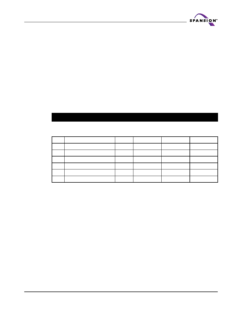
Table 7.15. Chip Erase
(LLD Function = lld_ChipEraseCmd)
Cycle
Description
Operation
Byte Address
Word Address
Data
1
Unlock
Write
Base + AAAh
Base + 555h
00AAh
2
Unlock
Write
Base + 554h
Base + 2AAh
0055h
3
Setup Command
Write
Base + AAAh
Base + 555h
0080h
4
Unlock
Write
Base + AAAh
Base + 555h
00AAh
5
Unlock
Write
Base + 554h
Base + 2AAh
0055h
6
Chip Erase Command
Write
Base + AAAh
Base + 555h
0010h
相关PDF资料 |
PDF描述 |
|---|---|
| S29WS128N0LBFI111 | 256/128/64 MEGABIT CMOS 1.8 VOLT ONLY SIMULTANEOUS READ/WRITE BURST MODE FLASH MEMORY |
| S29WS128N0LBFI112 | 256/128/64 MEGABIT CMOS 1.8 VOLT ONLY SIMULTANEOUS READ/WRITE BURST MODE FLASH MEMORY |
| S29WS128N0LBFI113 | 256/128/64 MEGABIT CMOS 1.8 VOLT ONLY SIMULTANEOUS READ/WRITE BURST MODE FLASH MEMORY |
| S29WS128N0LBFW011 | Test Clip; Current Rating:100A; Body Material:Steel; Features:Unmarked; Jaw Opening Max:1.625"; Overall Length:6" RoHS Compliant: NA |
| S29WS128N0LBFI011 | 256/128/64 MEGABIT CMOS 1.8 VOLT ONLY SIMULTANEOUS READ/WRITE BURST MODE FLASH MEMORY |
相关代理商/技术参数 |
参数描述 |
|---|---|
| S29WS064N0PBAW012 | 制造商:SPANSION 制造商全称:SPANSION 功能描述:256/128/64 Megabit (16/8/4 M x 16-Bit) CMOS 1.8 Volt-only Simultaneous Read/Write, Burst Mode Flash Memory |
| S29WS064N0PBAW013 | 制造商:SPANSION 制造商全称:SPANSION 功能描述:256/128/64 MEGABIT CMOS 1.8 VOLT ONLY SIMULTANEOUS READ/WRITE BURST MODE FLASH MEMORY |
| S29WS064N0PBAW110 | 制造商:SPANSION 制造商全称:SPANSION 功能描述:256/128/64 MEGABIT CMOS 1.8 VOLT ONLY SIMULTANEOUS READ/WRITE BURST MODE FLASH MEMORY |
| S29WS064N0PBAW111 | 制造商:SPANSION 制造商全称:SPANSION 功能描述:256/128/64 MEGABIT CMOS 1.8 VOLT ONLY SIMULTANEOUS READ/WRITE BURST MODE FLASH MEMORY |
| S29WS064N0PBAW112 | 制造商:SPANSION 制造商全称:SPANSION 功能描述:256/128/64 MEGABIT CMOS 1.8 VOLT ONLY SIMULTANEOUS READ/WRITE BURST MODE FLASH MEMORY |
发布紧急采购,3分钟左右您将得到回复。