- 您现在的位置:买卖IC网 > PDF目录225141 > S29WS064N0PBAW011 (Spansion Inc.) 256/128/64 MEGABIT CMOS 1.8 VOLT ONLY SIMULTANEOUS READ/WRITE BURST MODE FLASH MEMORY PDF资料下载
参数资料
| 型号: | S29WS064N0PBAW011 |
| 厂商: | Spansion Inc. |
| 英文描述: | 256/128/64 MEGABIT CMOS 1.8 VOLT ONLY SIMULTANEOUS READ/WRITE BURST MODE FLASH MEMORY |
| 中文描述: | 256/128/64兆位的CMOS 1.8伏只有同时读/写突发模式闪存 |
| 文件页数: | 38/99页 |
| 文件大小: | 1091K |
| 代理商: | S29WS064N0PBAW011 |
第1页第2页第3页第4页第5页第6页第7页第8页第9页第10页第11页第12页第13页第14页第15页第16页第17页第18页第19页第20页第21页第22页第23页第24页第25页第26页第27页第28页第29页第30页第31页第32页第33页第34页第35页第36页第37页当前第38页第39页第40页第41页第42页第43页第44页第45页第46页第47页第48页第49页第50页第51页第52页第53页第54页第55页第56页第57页第58页第59页第60页第61页第62页第63页第64页第65页第66页第67页第68页第69页第70页第71页第72页第73页第74页第75页第76页第77页第78页第79页第80页第81页第82页第83页第84页第85页第86页第87页第88页第89页第90页第91页第92页第93页第94页第95页第96页第97页第98页第99页
January 25, 2005 S29WS-N_00_G0
41
Ad vance
Information
/* Example: Unlock Bypass Program Command
*/
/* Do while in Unlock Bypass Entry Mode!
*/
*( (UINT16 *)bank_addr + 0x555 ) = 0x00A0;
/* write program setup command
*/
*( (UINT16 *)pa )
= data;
/* write data to be programmed
*/
/* Poll until done or error.
*/
/* If done and more to program, */
/* do above two cycles again.
*/
/* Example: Unlock Bypass Exit Command */
*( (UINT16 *)base_addr + 0x000 ) = 0x0090;
*( (UINT16 *)base_addr + 0x000 ) = 0x0000;
7.5.9 Write Operation Status
The device provides several bits to determine the status of a program or erase operation. The
following subsections describe the function of DQ1, DQ2, DQ3, DQ5, DQ6, and DQ7.
DQ7: Data# Polling.
The Data# Polling bit, DQ7, indicates to the host system whether an Em-
bedded Program or Erase algorithm is in progress or completed, or whether a bank is in Erase
Suspend. Data# Polling is valid after the rising edge of the final WE# pulse in the command se-
quence. Note that the Data# Polling is valid only for the last word being programmed in the write-
buffer-page during Write Buffer Programming. Reading Data# Polling status on any word other
than the last word to be programmed in the write-buffer-page returns false status information.
During the Embedded Program algorithm, the device outputs on DQ7 the complement of the
datum programmed to DQ7. This DQ7 status also applies to programming during Erase Suspend.
When the Embedded Program algorithm is complete, the device outputs the datum programmed
to DQ7. The system must provide the program address to read valid status information on DQ7.
If a program address falls within a protected sector, Data# polling on DQ7 is active for approxi-
mately tPSP, then that bank returns to the read mode.
During the Embedded Erase Algorithm, Data# polling produces a “0” on DQ7. When the Embed-
ded Erase algorithm is complete, or if the bank enters the Erase Suspend mode, Data# Polling
produces a “1” on DQ7. The system must provide an address within any of the sectors selected
for erasure to read valid status information on DQ7.
After an erase command sequence is written, if all sectors selected for erasing are protected,
Data# Polling on DQ7 is active for approximately tASP, then the bank returns to the read mode.
If not all selected sectors are protected, the Embedded Erase algorithm erases the unprotected
sectors, and ignores the selected sectors that are protected. However, if the system reads DQ7
at an address within a protected sector, the status may not be valid.
Just prior to the completion of an Embedded Program or Erase operation, DQ7 may change asyn-
chronously with DQ6-DQ0 while Output Enable (OE#) is asserted low. That is, the device may
change from providing status information to valid data on DQ7. Depending on when the system
samples the DQ7 output, it may read the status or valid data. Even if the device has completed
2
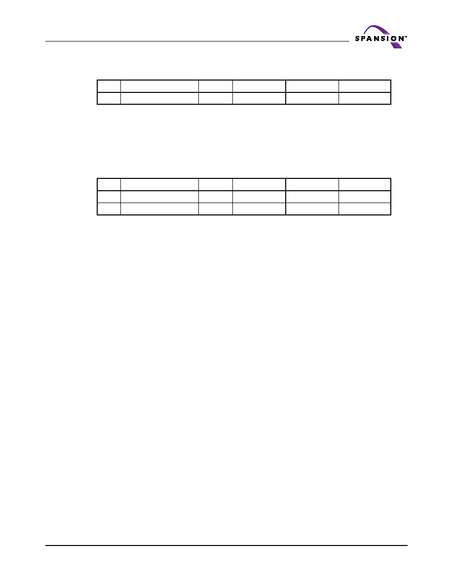
Program Command
Write
Program Address
Program Data
Table 7.22. Unlock Bypass Reset
(LLD Function = lld_UnlockBypassResetCmd)
Cycle
Description
Operation
Byte Address
Word Address
Data
1
Reset Cycle 1
Write
Base + xxxh
Base +xxxh
0090h
2
Reset Cycle 2
Write
Base + xxxh
Base +xxxh
0000h
Table 7.21. Unlock Bypass Program
(LLD Function = lld_UnlockBypassProgramCmd)
Cycle
Description
Operation
Byte Address
Word Address
Data
相关PDF资料 |
PDF描述 |
|---|---|
| S29WS128N0LBFI111 | 256/128/64 MEGABIT CMOS 1.8 VOLT ONLY SIMULTANEOUS READ/WRITE BURST MODE FLASH MEMORY |
| S29WS128N0LBFI112 | 256/128/64 MEGABIT CMOS 1.8 VOLT ONLY SIMULTANEOUS READ/WRITE BURST MODE FLASH MEMORY |
| S29WS128N0LBFI113 | 256/128/64 MEGABIT CMOS 1.8 VOLT ONLY SIMULTANEOUS READ/WRITE BURST MODE FLASH MEMORY |
| S29WS128N0LBFW011 | Test Clip; Current Rating:100A; Body Material:Steel; Features:Unmarked; Jaw Opening Max:1.625"; Overall Length:6" RoHS Compliant: NA |
| S29WS128N0LBFI011 | 256/128/64 MEGABIT CMOS 1.8 VOLT ONLY SIMULTANEOUS READ/WRITE BURST MODE FLASH MEMORY |
相关代理商/技术参数 |
参数描述 |
|---|---|
| S29WS064N0PBAW012 | 制造商:SPANSION 制造商全称:SPANSION 功能描述:256/128/64 Megabit (16/8/4 M x 16-Bit) CMOS 1.8 Volt-only Simultaneous Read/Write, Burst Mode Flash Memory |
| S29WS064N0PBAW013 | 制造商:SPANSION 制造商全称:SPANSION 功能描述:256/128/64 MEGABIT CMOS 1.8 VOLT ONLY SIMULTANEOUS READ/WRITE BURST MODE FLASH MEMORY |
| S29WS064N0PBAW110 | 制造商:SPANSION 制造商全称:SPANSION 功能描述:256/128/64 MEGABIT CMOS 1.8 VOLT ONLY SIMULTANEOUS READ/WRITE BURST MODE FLASH MEMORY |
| S29WS064N0PBAW111 | 制造商:SPANSION 制造商全称:SPANSION 功能描述:256/128/64 MEGABIT CMOS 1.8 VOLT ONLY SIMULTANEOUS READ/WRITE BURST MODE FLASH MEMORY |
| S29WS064N0PBAW112 | 制造商:SPANSION 制造商全称:SPANSION 功能描述:256/128/64 MEGABIT CMOS 1.8 VOLT ONLY SIMULTANEOUS READ/WRITE BURST MODE FLASH MEMORY |
发布紧急采购,3分钟左右您将得到回复。