- 您现在的位置:买卖IC网 > PDF目录225141 > S29WS064N0PBAW011 (Spansion Inc.) 256/128/64 MEGABIT CMOS 1.8 VOLT ONLY SIMULTANEOUS READ/WRITE BURST MODE FLASH MEMORY PDF资料下载
参数资料
| 型号: | S29WS064N0PBAW011 |
| 厂商: | Spansion Inc. |
| 英文描述: | 256/128/64 MEGABIT CMOS 1.8 VOLT ONLY SIMULTANEOUS READ/WRITE BURST MODE FLASH MEMORY |
| 中文描述: | 256/128/64兆位的CMOS 1.8伏只有同时读/写突发模式闪存 |
| 文件页数: | 90/99页 |
| 文件大小: | 1091K |
| 代理商: | S29WS064N0PBAW011 |
第1页第2页第3页第4页第5页第6页第7页第8页第9页第10页第11页第12页第13页第14页第15页第16页第17页第18页第19页第20页第21页第22页第23页第24页第25页第26页第27页第28页第29页第30页第31页第32页第33页第34页第35页第36页第37页第38页第39页第40页第41页第42页第43页第44页第45页第46页第47页第48页第49页第50页第51页第52页第53页第54页第55页第56页第57页第58页第59页第60页第61页第62页第63页第64页第65页第66页第67页第68页第69页第70页第71页第72页第73页第74页第75页第76页第77页第78页第79页第80页第81页第82页第83页第84页第85页第86页第87页第88页第89页当前第90页第91页第92页第93页第94页第95页第96页第97页第98页第99页
88
S29WS-N_00_G0 January 25, 2005
Adva nce
Information
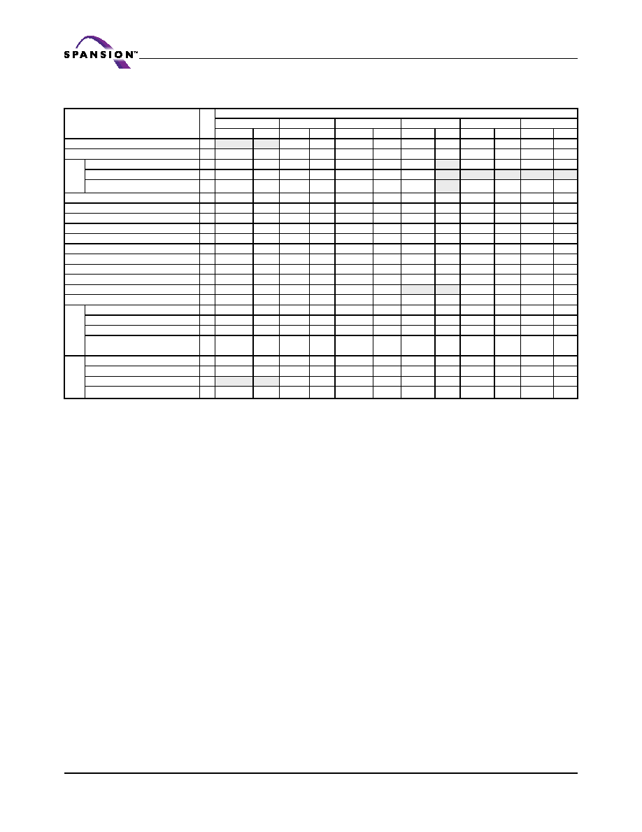
Table 12.1.
Memory Array Commands
Command Sequence
(Notes)
Cy
cl
es
Bus Cycles (Notes 1–5)
First
Second
Third
Fourth
Fifth
Sixth
Addr
Data
Addr
Data
Addr
Data
Addr
Data
Addr
Data
Addr
Data
Asynchronous Read (6)
1
RA
RD
Reset (7)
1
XXX
F0
Aut
o-
sel
ect
(8)
Manufacturer ID
4
555
AA
2AA
55
[BA]555
90
[BA]X00
0001
Device ID (9)
6
555
AA
2AA
55
[BA]555
90
[BA]X01
227E
BA+X0E
Data
BA+X0F 2200
Indicator Bits (10)
4
555
AA
2AA
55
[BA]555
90
[BA]X03
Data
Program
4
555
AA
2AA
55
555
A0
PA
PD
Write to Buffer (11)
6
555
AA
2AA
55
PA
25
PA
WC
PA
PD
WBL
PD
Program Buffer to Flash
1
SA
29
Write to Buffer Abort Reset (12)
3
555
AA
2AA
55
555
F0
Chip Erase
6
555
AA
2AA
55
555
80
555
AA
2AA
55
555
10
Sector Erase
6
555
AA
2AA
55
555
80
555
AA
2AA
55
SA
30
Erase/Program Suspend (13)
1
BA
B0
Erase/Program Resume (14)
1
BA
30
Set Configuration Register (18)
4
555
AA
2AA
55
555
D0
X00
CR
Read Configuration Register
4
555
AA
2AA
55
555
C6
X00
CR
CFI Query (15)
1
[BA]555
98
Unlock
Byp
ass
Mode
Entry
3
555
AA
2AA
55
555
20
Program (16)
2
XXX
A0
PA
PD
CFI (16)
1
XXX
98
Reset
2
XXX
90
XXX
00
SecSi
S
ect
or
Entry
3
555
AA
2AA
55
555
88
Program (17)
4
555
AA
2AA
55
555
A0
PA
PD
Read (17)
1
00
Data
Exit (17)
4
555
AA
2AA
55
555
90
XXX
00
Legend:
X = Don’t care.
RA = Read Address.
RD = Read Data.
PA = Program Address. Addresses latch on the rising edge of the
AVD# pulse or active edge of CLK, whichever occurs first.
PD = Program Data. Data latches on the rising edge of WE# or CE#
pulse, whichever occurs first.
SA = Sector Address. WS256N = A23–A14; WS128N = A22–A14;
WS064N = A21–A14.
BA = Bank Address. WS256N = A23–A20; WS128N = A22–A20;
WS064N = A21–A18.
CR = Configuration Register data bits D15–D0.
WBL = Write Buffer Location. Address must be within the same write
buffer page as PA.
WC = Word Count. Number of write buffer locations to load minus 1.
Notes:
1. See Table 7.1 for description of bus operations.
2. All values are in hexadecimal.
3. Shaded cells indicate read cycles.
4. Address and data bits not specified in table, legend, or notes are
don’t cares (each hex digit implies 4 bits of data).
5. Writing incorrect address and data values or writing them in the
improper sequence may place the device in an unknown state.
The system must write the reset command to return the device
to reading array data.
6. No unlock or command cycles required when bank is reading
array data.
7. Reset command is required to return to reading array data (or to
the erase-suspend-read mode if previously in Erase Suspend)
when a bank is in the autoselect mode, or if DQ5 goes high
(while the bank is providing status information) or performing
sector lock/unlock.
8. The system must provide the bank address. See Autoselect
section for more information.
9. Data in cycle 5 is 2230 (WS256N), 2232 (WS064N), or 2231
(WS128N).
10. See Table 7.9 for indicator bit values.
11. Total number of cycles in the command sequence is determined
by the number of words written to the write buffer.
12. Command sequence resets device for next command after write-
to-buffer operation.
13. System may read and program in non-erasing sectors, or enter
the autoselect mode, when in the Erase Suspend mode. The
Erase Suspend command is valid only during a sector erase
operation, and requires the bank address.
14. Erase Resume command is valid only during the Erase Suspend
mode, and requires the bank address.
15. Command is valid when device is ready to read array data or
when device is in autoselect mode. Address equals 55h on all
future devices, but 555h for WS256N/128N/064N.
16. Requires Entry command sequence prior to execution. Unlock
Bypass Reset command is required to return to reading array
data.
17. Requires Entry command sequence prior to execution. SecSi
Sector Exit Reset command is required to exit this mode; device
may otherwise be placed in an unknown state.
18. Requires reset command to configure the Configuration Register.
相关PDF资料 |
PDF描述 |
|---|---|
| S29WS128N0LBFI111 | 256/128/64 MEGABIT CMOS 1.8 VOLT ONLY SIMULTANEOUS READ/WRITE BURST MODE FLASH MEMORY |
| S29WS128N0LBFI112 | 256/128/64 MEGABIT CMOS 1.8 VOLT ONLY SIMULTANEOUS READ/WRITE BURST MODE FLASH MEMORY |
| S29WS128N0LBFI113 | 256/128/64 MEGABIT CMOS 1.8 VOLT ONLY SIMULTANEOUS READ/WRITE BURST MODE FLASH MEMORY |
| S29WS128N0LBFW011 | Test Clip; Current Rating:100A; Body Material:Steel; Features:Unmarked; Jaw Opening Max:1.625"; Overall Length:6" RoHS Compliant: NA |
| S29WS128N0LBFI011 | 256/128/64 MEGABIT CMOS 1.8 VOLT ONLY SIMULTANEOUS READ/WRITE BURST MODE FLASH MEMORY |
相关代理商/技术参数 |
参数描述 |
|---|---|
| S29WS064N0PBAW012 | 制造商:SPANSION 制造商全称:SPANSION 功能描述:256/128/64 Megabit (16/8/4 M x 16-Bit) CMOS 1.8 Volt-only Simultaneous Read/Write, Burst Mode Flash Memory |
| S29WS064N0PBAW013 | 制造商:SPANSION 制造商全称:SPANSION 功能描述:256/128/64 MEGABIT CMOS 1.8 VOLT ONLY SIMULTANEOUS READ/WRITE BURST MODE FLASH MEMORY |
| S29WS064N0PBAW110 | 制造商:SPANSION 制造商全称:SPANSION 功能描述:256/128/64 MEGABIT CMOS 1.8 VOLT ONLY SIMULTANEOUS READ/WRITE BURST MODE FLASH MEMORY |
| S29WS064N0PBAW111 | 制造商:SPANSION 制造商全称:SPANSION 功能描述:256/128/64 MEGABIT CMOS 1.8 VOLT ONLY SIMULTANEOUS READ/WRITE BURST MODE FLASH MEMORY |
| S29WS064N0PBAW112 | 制造商:SPANSION 制造商全称:SPANSION 功能描述:256/128/64 MEGABIT CMOS 1.8 VOLT ONLY SIMULTANEOUS READ/WRITE BURST MODE FLASH MEMORY |
发布紧急采购,3分钟左右您将得到回复。