- 您现在的位置:买卖IC网 > PDF目录21888 > SFCF8192H4BK4SA-I-QT-553-SMA (Swissbit NA Inc)FLASH SLC UDMA/MDMA/PIO 8G PDF资料下载
参数资料
| 型号: | SFCF8192H4BK4SA-I-QT-553-SMA |
| 厂商: | Swissbit NA Inc |
| 文件页数: | 33/99页 |
| 文件大小: | 0K |
| 描述: | FLASH SLC UDMA/MDMA/PIO 8G |
| 视频文件: | Swissbit Manufacturing Overview |
| RoHS指令信息: | Environment Protection Declaration |
| 标准包装: | 20 |
| 系列: | C-300 |
| 存储容量: | 8GB |
| 存储器类型: | CompactFlash? |
| 其它名称: | 1052-1012 |
第1页第2页第3页第4页第5页第6页第7页第8页第9页第10页第11页第12页第13页第14页第15页第16页第17页第18页第19页第20页第21页第22页第23页第24页第25页第26页第27页第28页第29页第30页第31页第32页当前第33页第34页第35页第36页第37页第38页第39页第40页第41页第42页第43页第44页第45页第46页第47页第48页第49页第50页第51页第52页第53页第54页第55页第56页第57页第58页第59页第60页第61页第62页第63页第64页第65页第66页第67页第68页第69页第70页第71页第72页第73页第74页第75页第76页第77页第78页第79页第80页第81页第82页第83页第84页第85页第86页第87页第88页第89页第90页第91页第92页第93页第94页第95页第96页第97页第98页第99页
�� �
�
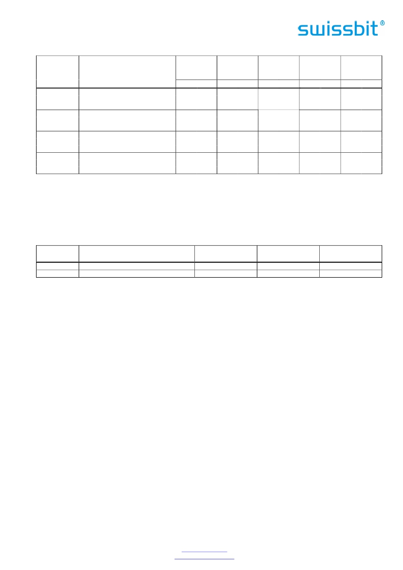
�Table 28: Ultr� a� DMA� Sender� and� Recipient� IC� Timing� Requirements�
�Name�
�Comments�
�UDMA�
�Mode� 0�
�(ns)�
�UDMA�
�Mode� 1�
�(ns)�
�UDMA�
�Mode� 2�
�(ns)�
�UDMA�
�Mode� 3�
�(ns)�
�UDMA�
�Mode4�
�(ns)�
�Min�
�Max�
�Min�
�Max�
�Min�
�Max�
�Min�
�Max�
�Min�
�Max�
�t� DSIC�
�Recipient� IC� data� setup� time� (from�
�14.7�
�9.7�
�6.8�
�6.8�
�4.8�
�data� valid� until� STROBE� edge)�
�(see� note� 2)�
�t� DHIC�
�Recipient� IC� data� hold� time� (from�
�4.8�
�4.8�
�4.8�
�4.8�
�4.8�
�STROBE� edge� until� data� may�
�become� invalid)� (see� note� 2)�
�t� DVSIC�
�Sender� IC� data� valid� setup� time�
�72.9�
�50.9�
�33.9�
�22.6�
�9.5�
�(from� data� valid� until� STROBE�
�edge)� (see� note� 3)�
�t� DVHIC�
�Sender� IC� data� valid� hold� time�
�9.0�
�9.0�
�9.0�
�9.0�
�9.0�
�(from� STROBE� edge� until� data�
�may� become� invalid)� (see� note� 3)�
�Notes:�
�1.�
�2.�
�3.�
�All� timing� measurement� switching� points(low� to� high� and� high� to� low)� shall� be� taken� at� 1.5� V.�
�The� correct� data� value� shall� be� captured� by� the� recipient� given� input� data� with� a� slew� rate� of� 0.4� V/ns� rising� and� falling�
�and� the� input� STROBE� with� a� slew� rate� of� 0.4� V/ns� rising� and� falling� at� t� DSIC� and� t� DHIC� timing� (as� measured� through� 1.5�
�V).�
�The� parameters� t� DVSIC� and� t� DVHIC� shall� be� met� for� lumped� capacitive� loads� of� 15� and� 40� pF� at� the� IC� where� all� signals�
�have� the� same� capacitive� load� value.� Noise� that� may� couple� onto� the� output� signals� from� external� sources� has� not� been�
�included� in� these� values.�
�Table 29: Ultr� a� DMA� AC� Signal� Requirements�
�Name�
�Comment�
�Min�
�Max�
�Notes�
�[V/ns]�
�[V/ns]�
�S� RISE�
�S� FALL�
�Rising� Edge� Slew� Rate� for� any� signal�
�Falling� Edge� Slew� Rate� for� any� signal�
�1.25�
�1.25�
�1�
�1�
�Note:�
�1.�
�The� sender� shall� be� tested� while� driving� an� 18� inch� long,� 80� conductor� cable� with� PVC� insulation� material.� The� signal�
�under� test� shall� be� cut� at� a� test� point� so� that� it� has� not� trace,� cable� or� recipient� loading� after� the� test� point.� All� other�
�signals� should� remain� connected� through� to� the� recipient.� The� test� point� may� be� located� at� any� point� between� the�
�sender’s� series� termination� resistor� and� one� half� inch� or� less� of� conductor� exiting� the� connector.� If� the� test� point� is� on�
�a� cable� conductor� rather� than� the� PCB,� an� adjacent� ground� conductor� shall� also� be� cut� within� one� half� inch� of� the�
�connector.�
�The� test� load� and� test� points� should� then� be� soldered� directly� to� the� exposed� source� side� connectors.� The� test� loads�
�consist� of� a� 15� pF� or� a� 40� pF,� 5%,� 0.08� inch� by� 0.05� inch� surface� mount� or� smaller� size� capacitor� from� the� test� point� to�
�ground.� Slew� rates� shall� be� met� for� both� capacitor� values.�
�Measurements� shall� be� taken� at� the� test� point� using� a� <1� pF,� >100� Kohm,� 1� Ghz� or� faster� probe� and� a� 500� MHz� or�
�faster� oscilloscope.� The� average� rate� shall� be� measured� from� 20%� to� 80%� of� the� settled� VOH� level� with� data�
�transitions� at� least� 120� ns� apart.� The� settled� VOH� level� shall� be� measured� as� the� average� output� high� level� under� the�
�defined� testing� conditions� from� 100� nsec� after� 80%� of� a� rising� edge� until� 20%� of� the� subsequent� falling� edge.�
�6.5.4.4.1� Initiating� an� Ultra� DMA� Data-In� Burst�
�a)� An� Ultra� DMA� Data-In� burst� is� initiated� by� following� the� steps� lettered� below.� The� timing� diagram� is�
�shown� in� Figure� 10:� Ultra� DMA� Data-In� Burst� Initiation� Timing.� The� associated� timing� parameters� are�
�specified� in� Table� 26:� Ultra� DMA� Data� Burst� Timing� Requirements� and� are� described� in� Table� 27:� Ultra� DMA�
��b)� The� following� steps� shall� occur� in� the� order� they� are� listed� unless� otherwise� specifically� allowed:�
�c)�
�The� host� shall� keep� –� DMACK� in� the� negated� state� before� an� Ultra� DMA� burst� is� initiated.�
�d)� The� device� shall� assert� DMARQ� to� initiate� an� Ultra� DMA� burst.� After� assertion� of� DMARQ� the� device� shall� not�
�negate� DMARQ� until� after� the� first� negation� of� DSTROBE.�
�e)� Steps� I,� (d),� and� (e)� may� occur� in� any� order� or� at� the� same� time.� The� host� shall� assert� STOP.�
�f)�
�The� host� shall� negate� –� HDMARDY.�
�g)� The� host� shall� negate� –� CS0,� -CS1,� DA2,� DA1,� and� DA0.� The� host� shall� keep� –� CS0,� -CS1,� DA2,� DA1,� and� DA0�
�negated� until� after� negating� –� DMACK� at� the� end� of� the� burst.�
�h)� Steps� I,� (d),� and� (e)� shall� have� occurred� at� least� t� ACK� before� the� host� asserts� –� DMACK.� The� host� shall� keep� –�
�DMACK� asserted� until� the� end� of� an� Ultra� DMA� burst.�
�i)�
�j)�
�The� host� shall� release� D[15:00]� within� t� AZ� after� asserting� –� DMACK.�
�The� device� may� assert� DSTROBE� t� ZIORDY� after� the� host� has� asserted� –� DMACK.� Once� the� device� has� driven�
�DSTROBE� the� device� shall� not� release� DSTROBE� until� after� the� host� has� negated� –� DMACK� at� the� end� of� an�
�Ultra� DMA� burst.�
�Swissbit� AG�
�Industriestrasse� 4�
�Swissbit� reserves� the� right� to� change� products� or� specifications� without� notice.�
�Revision:� 1.51�
�CH-9552� Bronschhofen�
�Switzerland�
�www.swissbit.com�
�industrial@swissbit.com�
�C-300_data_sheet_CF-HxBK_Rev151.doc�
�Page� 33� of� 99�
�相关PDF资料 |
PDF描述 |
|---|---|
| TSL245R-LF | IC LIGHT TO FREQUENCY CONV 3PIN |
| TSL235R-LF | IC LIGHT TO FREQUENCY CONV 3PIN |
| SFCF4096H1BO2TO-I-D1-523-SMA | FLASH SLC UDMA/MDMA/PIO 4G |
| MLBAWT-A1-0000-0000DZ | LED XLAMP ML-B WHITE SMD |
| MLBAWT-A1-0000-0000DV | LED XLAMP ML-B WHITE SMD |
相关代理商/技术参数 |
参数描述 |
|---|---|
| SFC-FUSE-CAB | 功能描述:熔丝座配件 SFC-FUSE-CAB RoHS:否 制造商:Schurter 产品:Caps 类型:Slot Knob 用于:FEU, FEU (Med), FAU, FAC |
| SFC-HC | 制造商:PANASONIC ELECTRIC WORKS ACSD 功能描述:Handy Controller For SF4C Series Only 制造商:PANASONIC ELECTRIC WORKS - ACSD 功能描述:HANDY CONTROLLER FOR SF4C |
| SFCIC5000102MX1 | 功能描述:电磁干扰直通滤波器 500V .001uF X7R 20% C Filter RoHS:否 制造商:Tusonix 电容:0.027 uF 电压额定值:50 V 电路类型: 最大直流电流: 最大直流电阻: 工作温度范围:- 55 C to + 125 C 系列:4403 螺纹大小:4-40 UNC-2A |
| SFCIC5000103MX1 | 功能描述:电磁干扰直通滤波器 500V .01uF X7R C FILTER W/NUTS RoHS:否 制造商:Tusonix 电容:0.027 uF 电压额定值:50 V 电路类型: 最大直流电流: 最大直流电阻: 工作温度范围:- 55 C to + 125 C 系列:4403 螺纹大小:4-40 UNC-2A |
| SFCIC5000220ZC1 | 功能描述:电磁干扰直通滤波器 500V 22pF C0G C FILTER W/NUTS RoHS:否 制造商:Tusonix 电容:0.027 uF 电压额定值:50 V 电路类型: 最大直流电流: 最大直流电阻: 工作温度范围:- 55 C to + 125 C 系列:4403 螺纹大小:4-40 UNC-2A |
发布紧急采购,3分钟左右您将得到回复。