- 您现在的位置:买卖IC网 > PDF目录98145 > ST72E85A5G0 (STMICROELECTRONICS) 8-BIT, UVPROM, 4.332 MHz, MICROCONTROLLER, CQFP80 PDF资料下载
参数资料
| 型号: | ST72E85A5G0 |
| 厂商: | STMICROELECTRONICS |
| 元件分类: | 微控制器/微处理器 |
| 英文描述: | 8-BIT, UVPROM, 4.332 MHz, MICROCONTROLLER, CQFP80 |
| 封装: | WINDOWED, CERAMIC, QFP- 80 |
| 文件页数: | 56/117页 |
| 文件大小: | 748K |
| 代理商: | ST72E85A5G0 |
第1页第2页第3页第4页第5页第6页第7页第8页第9页第10页第11页第12页第13页第14页第15页第16页第17页第18页第19页第20页第21页第22页第23页第24页第25页第26页第27页第28页第29页第30页第31页第32页第33页第34页第35页第36页第37页第38页第39页第40页第41页第42页第43页第44页第45页第46页第47页第48页第49页第50页第51页第52页第53页第54页第55页当前第56页第57页第58页第59页第60页第61页第62页第63页第64页第65页第66页第67页第68页第69页第70页第71页第72页第73页第74页第75页第76页第77页第78页第79页第80页第81页第82页第83页第84页第85页第86页第87页第88页第89页第90页第91页第92页第93页第94页第95页第96页第97页第98页第99页第100页第101页第102页第103页第104页第105页第106页第107页第108页第109页第110页第111页第112页第113页第114页第115页第116页第117页
43/117
ST7285C
16-BIT TIMER (Cont’d)
4.3.6 Timer Registers
As can be seen from the Memory Map, each Timer
is associated with three control and status regis-
ters which are described in detail below, as well as
with six pairs of data registers (16-bit values) relat-
ing to the two input captures, the two output com-
pares, the counter and the alternate counter.
These six pairs of data registers are self-explana-
tory and need no further description.
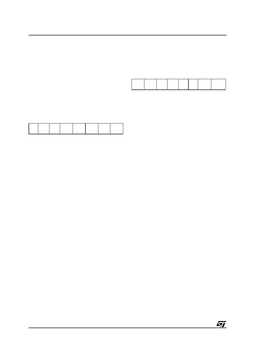
TIMER CONTROL REGISTER 1 (TCR1)
Address: see Memory Map
—
Read/Write
Reset Value: 0000 0000b
Bit 7 = ICIE
Input Capture Interrupt Enable
If ICIE is set, a timer interrupt is enabled whenever
the ICF1 or ICF2 status flags of TSR are set. If the
ICIE bit is cleared, the interrupt is inhibited.
Bit 6 = OCIE
Output Compare Interrupt Enable
If OCIE is set, a timer interrupt is enabled whenev-
er the OCF1 or OCF2 status flags of TSR are set.
If the OCIE bit is cleared, the interrupt is inhibited.
Bit 5 = TOIE
Timer Overflow Interrupt Enable
If TOIE is set, a timer interrupt is enable whenever
the TOF status flag of TSR is set. If the TOIE bit is
cleared, the interrupt is inhibited.
Bit 4 = FOLV2
Forced Output Compare 2
When written to 1, FOLV2 forces OLVL2 to be
copied to the OCMP2 pin. FOLV2 has no effect
otherwise. It can only be reset by a system reset.
Bit 3 = FOLV1
Forced Output Compare 1
When written to 1, FOLV1 forces OLVL1 to be
copied to the OCMP1 pin. FOLV1 has no effect
otherwise. It can only be reset by a System Reset.
Bit 2 = OLVL2 Output Level 2
The OLVL2 bit is copied to the OCMP2 pin when-
ever a successful comparison occurs at OCR2.
Bit 1 = IEDG1 Input Edge 1
The value of IEDG1 determines which type of level
transition on pin ICAP1 will trigger a free running
counter transfer to the ICR1. When IEDG1 is set, a
rising edge triggers the capture, and when it is re-
set, a falling edge does.
Bit 0 = OLVL1
Output Level 1
The OLVL1 bit is copied to the OCMP1 pin when-
ever a successful comparison occurs at OCR1.
TIMER CONTROL REGISTER 2 (TCR2)
Address: see Memory Map
—
Read/Write
Reset Value: 0000 0000b
Bit 7 = OC1E
Output Compare 1 Enable
If OC1E is set, the Output Compare 1 pin
(OCMP1) is dedicated to the output compare 1 ca-
pability of the timer. If OC1E is reset, this pin is a
general use I/O pin.
Bit 6 = OC2E
Output Compare 2 Enable
If OC2E is set, the output compare 2 pin (OCMP2)
is dedicated the output compare 2 capability of the
timer. If OC2E is reset, this is a general I/O pin.
Bit 5 = OPM
One Pulse Mode
If OPM is set, the input pin ICAP1 is usable to trig-
ger one pulse on the output pin OCMP1; the active
transition on ICAP1 is given by the state of IEDG1.
The length of the generated pulse depends on the
the contents of OCR1.
Bit 4 = PWM
Pulse Width Modulation
If PWM is set, the output pin OCMP1 outputs a
programmable cyclic signal; the length of the pulse
depends on the value of OCR1; the period de-
pends on the value of OCR2.
Bit 3, 2 = CC1-CC0
Clock Control
00: the internal clock is divided by 4
01: the internal clock is divided by 2
10: the internal clock is divided by 8
11: the external clock is selected as shown
in the Block Diagram.
Bit 1 = IEDG2 Input Edge 2
The value of IEDG2 determines which level transi-
tion on pin ICAP2 will trigger the free running
counter transfer to the ICR2. When IEDG2 is high,
a rising edge triggers the capture since when low,
a falling edge does.
Bit 0 = EXEDG
External Clock Edge
The status of EXEDG determines which type of
level transition on the external clock pin EXCLK
will trigger the free running counter. When EXEDG
is set, the active transition is the rising edge; when
EXEDG is reset, the active transition is the falling
edge.
70
ICIE
OCIE
TOIE FOLV2 FOLV1 OLVL2 IEDG1 OLVL1
70
OC1E
OC2E
OPM
PWM
CC1
CC0
IEDG2
EXEDG
相关PDF资料 |
PDF描述 |
|---|---|
| ST72F321J9T7 | 8-BIT, FLASH, 8 MHz, MICROCONTROLLER, PQFP44 |
| ST72F321J7T3 | 8-BIT, FLASH, 8 MHz, MICROCONTROLLER, PQFP44 |
| ST72F321J7T1 | 8-BIT, FLASH, 8 MHz, MICROCONTROLLER, PQFP44 |
| ST72F321J9T5 | 8-BIT, FLASH, 8 MHz, MICROCONTROLLER, PQFP44 |
| ST72F324BJ6B6 | 8-BIT, FLASH, 8 MHz, MICROCONTROLLER, PDIP42 |
相关代理商/技术参数 |
参数描述 |
|---|---|
| ST72F260G1B5 | 功能描述:8位微控制器 -MCU Flask 4K SPI RoHS:否 制造商:Silicon Labs 核心:8051 处理器系列:C8051F39x 数据总线宽度:8 bit 最大时钟频率:50 MHz 程序存储器大小:16 KB 数据 RAM 大小:1 KB 片上 ADC:Yes 工作电源电压:1.8 V to 3.6 V 工作温度范围:- 40 C to + 105 C 封装 / 箱体:QFN-20 安装风格:SMD/SMT |
| ST72F260G1M6 | 功能描述:8位微控制器 -MCU Flash 4K SPI/I2C/SCI RoHS:否 制造商:Silicon Labs 核心:8051 处理器系列:C8051F39x 数据总线宽度:8 bit 最大时钟频率:50 MHz 程序存储器大小:16 KB 数据 RAM 大小:1 KB 片上 ADC:Yes 工作电源电压:1.8 V to 3.6 V 工作温度范围:- 40 C to + 105 C 封装 / 箱体:QFN-20 安装风格:SMD/SMT |
| ST72F260G1M6/TR | 功能描述:8位微控制器 -MCU 8B MCU FLASH OR ROM MEMORY RoHS:否 制造商:Silicon Labs 核心:8051 处理器系列:C8051F39x 数据总线宽度:8 bit 最大时钟频率:50 MHz 程序存储器大小:16 KB 数据 RAM 大小:1 KB 片上 ADC:Yes 工作电源电压:1.8 V to 3.6 V 工作温度范围:- 40 C to + 105 C 封装 / 箱体:QFN-20 安装风格:SMD/SMT |
| ST72F262G1B5 | 功能描述:8位微控制器 -MCU Flask 4K SPI RoHS:否 制造商:Silicon Labs 核心:8051 处理器系列:C8051F39x 数据总线宽度:8 bit 最大时钟频率:50 MHz 程序存储器大小:16 KB 数据 RAM 大小:1 KB 片上 ADC:Yes 工作电源电压:1.8 V to 3.6 V 工作温度范围:- 40 C to + 105 C 封装 / 箱体:QFN-20 安装风格:SMD/SMT |
| ST72F262G1B6 | 功能描述:8位微控制器 -MCU 8B MCU RoHS:否 制造商:Silicon Labs 核心:8051 处理器系列:C8051F39x 数据总线宽度:8 bit 最大时钟频率:50 MHz 程序存储器大小:16 KB 数据 RAM 大小:1 KB 片上 ADC:Yes 工作电源电压:1.8 V to 3.6 V 工作温度范围:- 40 C to + 105 C 封装 / 箱体:QFN-20 安装风格:SMD/SMT |
发布紧急采购,3分钟左右您将得到回复。