- 您现在的位置:买卖IC网 > PDF目录98145 > ST72E85A5G0 (STMICROELECTRONICS) 8-BIT, UVPROM, 4.332 MHz, MICROCONTROLLER, CQFP80 PDF资料下载
参数资料
| 型号: | ST72E85A5G0 |
| 厂商: | STMICROELECTRONICS |
| 元件分类: | 微控制器/微处理器 |
| 英文描述: | 8-BIT, UVPROM, 4.332 MHz, MICROCONTROLLER, CQFP80 |
| 封装: | WINDOWED, CERAMIC, QFP- 80 |
| 文件页数: | 88/117页 |
| 文件大小: | 748K |
| 代理商: | ST72E85A5G0 |
第1页第2页第3页第4页第5页第6页第7页第8页第9页第10页第11页第12页第13页第14页第15页第16页第17页第18页第19页第20页第21页第22页第23页第24页第25页第26页第27页第28页第29页第30页第31页第32页第33页第34页第35页第36页第37页第38页第39页第40页第41页第42页第43页第44页第45页第46页第47页第48页第49页第50页第51页第52页第53页第54页第55页第56页第57页第58页第59页第60页第61页第62页第63页第64页第65页第66页第67页第68页第69页第70页第71页第72页第73页第74页第75页第76页第77页第78页第79页第80页第81页第82页第83页第84页第85页第86页第87页当前第88页第89页第90页第91页第92页第93页第94页第95页第96页第97页第98页第99页第100页第101页第102页第103页第104页第105页第106页第107页第108页第109页第110页第111页第112页第113页第114页第115页第116页第117页
72/117
ST7285C
4.9 RDS G.B.S
4.9.1 Introduction
The main task of the GBS module is to acquire
Group and Block Synchronization of a received
RDS data steam, which is provided in a modified
shortened cyclic code.
In order to achieve synchronization, a syndrome is
calculated on every data clock pulse. Detection of
a valid syndrome is indicated by flag VSI with as-
sociated interrupt, while the corresponding block is
kept in BL(0:2). Starting in BIT_SYNC mode the
SW can use CNA zero count interrupt (CNA=1)
and VSI check for synchronization phase. If the
synchronization criteria is fulfilled, the SW can
switch to BLK_SYNC mode, setting counter CNA
to 26 and CNB to the current block code. The SW
maintains block synchronization easily by check-
ing VSI and ORD, which indicates a correct block
order.
An optional GRP_SYNC mode can be entered for
RDS standby operation using the appropriate
counter interrupt selection.
The combination of software triggered syndrome
calculation, a second 26-bit shift register and a 26-
bit quality register, allow highly flexible error cor-
rection by software.
Single quality errors, representing a 1 or 2 bit
RDSDAT error, are indicated by the SQE flag.
They can be corrected by SW with high security.
4.9.2 Features
– Hardware implemented decoding of RDS data
stream.
– Hardware triggered syndrome calculation with
every rising edge of RDSCLK.
– Storage of 26 RDS bits (1 block).
– Fast syndrome calculation
(within 2.4
sat f
OSC=8.664MHz).
– 5-bits RDS-counter CNA and 2-bit RDS-block
counter CNB.
– Selectable counter interrupt for BIT/BLOCK/
GROUP-SYNC mode.
– “Valid Syndrome” detection unit with interrupt
and block code output.
– Selectable MMBS Radio Paging option for block
E syndrome detection.
– “Valid Block Order” flag.
– Extended “error correction by software” support.
– Software triggered syndrome calculation.
– Parallel storage of 26 RDSDAT bits and 26
QUALITY bits for high flexibility.
– Single/Multiple quality-error flags.
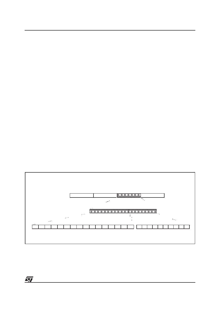
Figure 34. Principles of Baseband Coding
BLOCK1
BLOCK2
BLOCK3
BLOCK4
GROUP = 4 BLOCKS = 104 BITS
m15 m14 m13 m12 m11 m10 m9 m8 m7 m6 m5 m4 m3 m2 m1 m0
c9
’
c8
’
c7
’
c6
’
c5
’
c4
’
c3
’
c2
’
c1
’
c0
’
BLOCK = 26BITS
INFORMATION WORD = 16-BITS
CHECK WORD = 10-BITS
相关PDF资料 |
PDF描述 |
|---|---|
| ST72F321J9T7 | 8-BIT, FLASH, 8 MHz, MICROCONTROLLER, PQFP44 |
| ST72F321J7T3 | 8-BIT, FLASH, 8 MHz, MICROCONTROLLER, PQFP44 |
| ST72F321J7T1 | 8-BIT, FLASH, 8 MHz, MICROCONTROLLER, PQFP44 |
| ST72F321J9T5 | 8-BIT, FLASH, 8 MHz, MICROCONTROLLER, PQFP44 |
| ST72F324BJ6B6 | 8-BIT, FLASH, 8 MHz, MICROCONTROLLER, PDIP42 |
相关代理商/技术参数 |
参数描述 |
|---|---|
| ST72F260G1B5 | 功能描述:8位微控制器 -MCU Flask 4K SPI RoHS:否 制造商:Silicon Labs 核心:8051 处理器系列:C8051F39x 数据总线宽度:8 bit 最大时钟频率:50 MHz 程序存储器大小:16 KB 数据 RAM 大小:1 KB 片上 ADC:Yes 工作电源电压:1.8 V to 3.6 V 工作温度范围:- 40 C to + 105 C 封装 / 箱体:QFN-20 安装风格:SMD/SMT |
| ST72F260G1M6 | 功能描述:8位微控制器 -MCU Flash 4K SPI/I2C/SCI RoHS:否 制造商:Silicon Labs 核心:8051 处理器系列:C8051F39x 数据总线宽度:8 bit 最大时钟频率:50 MHz 程序存储器大小:16 KB 数据 RAM 大小:1 KB 片上 ADC:Yes 工作电源电压:1.8 V to 3.6 V 工作温度范围:- 40 C to + 105 C 封装 / 箱体:QFN-20 安装风格:SMD/SMT |
| ST72F260G1M6/TR | 功能描述:8位微控制器 -MCU 8B MCU FLASH OR ROM MEMORY RoHS:否 制造商:Silicon Labs 核心:8051 处理器系列:C8051F39x 数据总线宽度:8 bit 最大时钟频率:50 MHz 程序存储器大小:16 KB 数据 RAM 大小:1 KB 片上 ADC:Yes 工作电源电压:1.8 V to 3.6 V 工作温度范围:- 40 C to + 105 C 封装 / 箱体:QFN-20 安装风格:SMD/SMT |
| ST72F262G1B5 | 功能描述:8位微控制器 -MCU Flask 4K SPI RoHS:否 制造商:Silicon Labs 核心:8051 处理器系列:C8051F39x 数据总线宽度:8 bit 最大时钟频率:50 MHz 程序存储器大小:16 KB 数据 RAM 大小:1 KB 片上 ADC:Yes 工作电源电压:1.8 V to 3.6 V 工作温度范围:- 40 C to + 105 C 封装 / 箱体:QFN-20 安装风格:SMD/SMT |
| ST72F262G1B6 | 功能描述:8位微控制器 -MCU 8B MCU RoHS:否 制造商:Silicon Labs 核心:8051 处理器系列:C8051F39x 数据总线宽度:8 bit 最大时钟频率:50 MHz 程序存储器大小:16 KB 数据 RAM 大小:1 KB 片上 ADC:Yes 工作电源电压:1.8 V to 3.6 V 工作温度范围:- 40 C to + 105 C 封装 / 箱体:QFN-20 安装风格:SMD/SMT |
发布紧急采购,3分钟左右您将得到回复。