- 您现在的位置:买卖IC网 > PDF目录382636 > TMX20F2810PBKAEP (Texas Instruments, Inc.) Digital Signal Processors PDF资料下载
参数资料
| 型号: | TMX20F2810PBKAEP |
| 厂商: | Texas Instruments, Inc. |
| 元件分类: | 数字信号处理 |
| 英文描述: | Digital Signal Processors |
| 中文描述: | 数字信号处理器 |
| 文件页数: | 108/159页 |
| 文件大小: | 2084K |
| 代理商: | TMX20F2810PBKAEP |
第1页第2页第3页第4页第5页第6页第7页第8页第9页第10页第11页第12页第13页第14页第15页第16页第17页第18页第19页第20页第21页第22页第23页第24页第25页第26页第27页第28页第29页第30页第31页第32页第33页第34页第35页第36页第37页第38页第39页第40页第41页第42页第43页第44页第45页第46页第47页第48页第49页第50页第51页第52页第53页第54页第55页第56页第57页第58页第59页第60页第61页第62页第63页第64页第65页第66页第67页第68页第69页第70页第71页第72页第73页第74页第75页第76页第77页第78页第79页第80页第81页第82页第83页第84页第85页第86页第87页第88页第89页第90页第91页第92页第93页第94页第95页第96页第97页第98页第99页第100页第101页第102页第103页第104页第105页第106页第107页当前第108页第109页第110页第111页第112页第113页第114页第115页第116页第117页第118页第119页第120页第121页第122页第123页第124页第125页第126页第127页第128页第129页第130页第131页第132页第133页第134页第135页第136页第137页第138页第139页第140页第141页第142页第143页第144页第145页第146页第147页第148页第149页第150页第151页第152页第153页第154页第155页第156页第157页第158页第159页
Electrical Specifications
108
March 2004 Revised October 2004
SGUS051A
6.17
Event Manager Interface
6.17.1
PWM Timing
PWM refers to all PWM outputs on EVA and EVB.
Table 613. PWM Switching Characteristics
PARAMETER
TEST CONDITIONS
MIN
MAX
UNIT
tw(PWM)§
td(PWM)XCO
See the GPIO output timing for fall/rise times for PWM pins.
PWM pin toggling frequency is limited by the GPIO output buffer switching frequency (20 MHz).
§PWM outputs may be 100%, 0%, or increments of tc(HCO) with respect to the PWM period.
Table 614. Timer and Capture Unit Timing Requirements
#
Pulse duration, PWMx output high/low
25
ns
Delay time, XCLKOUT high to PWMx output switching
XCLKOUT = SYSCLKOUT/4
10
ns
MIN
MAX
UNIT
tw(TDIR)
Pulse duration, TDIRx low/high
Without input qualifier
2 * tc(SCO)
1 * tc(SCO) + IQT||
2 * tc(SCO)
1 * tc(SCO) + IQT||
40
cycles
With input qualifier
tw(CAP)
Pulse duration, CAPx input low/high
Without input qualifier
cycles
With input qualifier
tw(TCLKINL)
tw(TCLKINH)
tc(TCLKIN)
The QUALPRD bit field value can range from 0 (no qualification) through 0xFF (510 SYSCLKOUT cycles). The qualification sampling period is
2n SYSCLKOUT cycles, where “n” is the value stored in the QUALPRD bit field. As an example, when QUALPRD = 1, the qualification sampling
period is 1 x 2 = 2 SYSCLKOUT cycles (i.e., the input is sampled every 2 SYSCLKOUT cycles). Six such samples will be taken over five sampling
windows, each window being 2n SYSCLKOUT cycles. For QUALPRD = 1, the minimum width that is needed is 5 x 2 = 10 SYSCLKOUT cycles.
However, since the external signal is driven asynchronously, a 11-SYSCLKOUT-wide pulse ensures reliable recognition.
#Maximum input frequency to the QEP = min[HSPCLK/2, 20 MHz]
||Input Qualification Time (IQT) = [5 x QUALPRD x 2] * tc(SCO)
Pulse duration, TCLKINx low as a percentage of TCLKINx cycle time
60
%
Pulse duration, TCLKINx high as a percentage of TCLKINx cycle time
40
60
%
Cycle time, TCLKINx
4 * tc(HCO)
ns
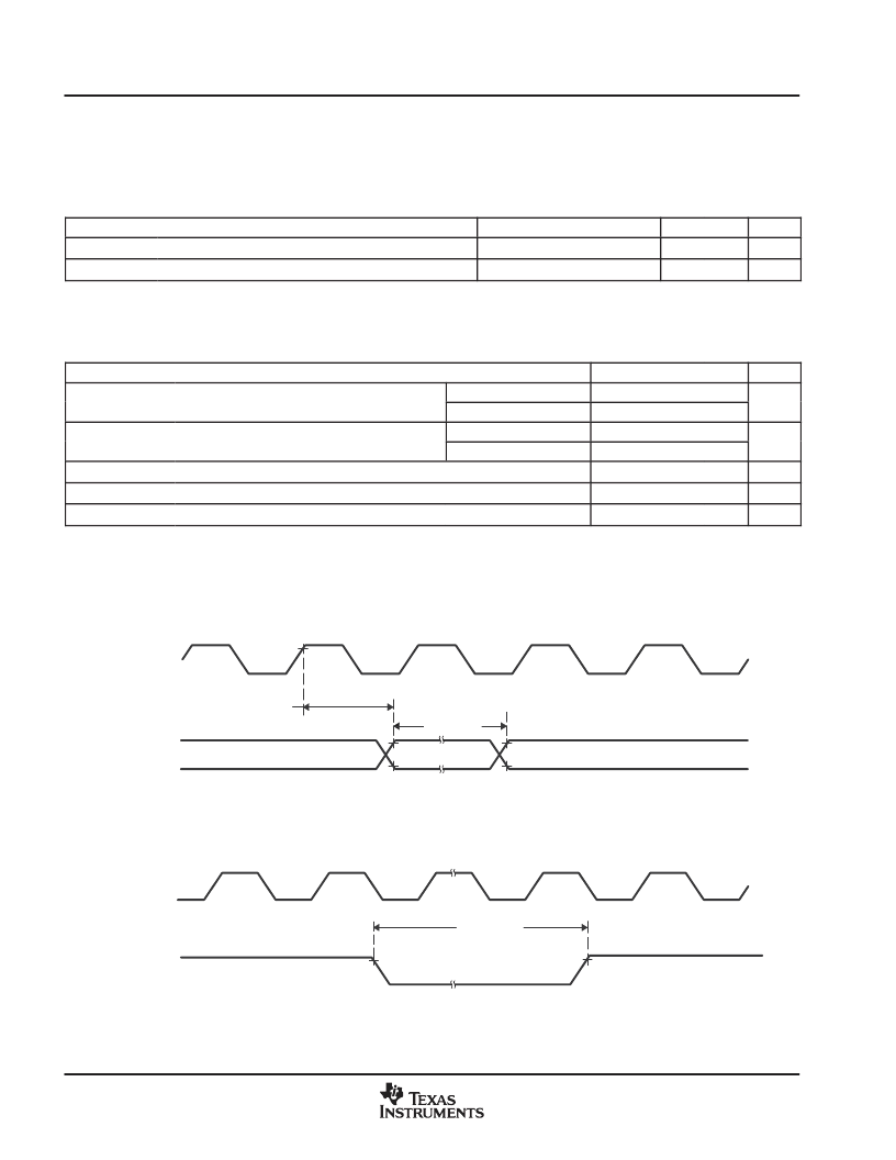
tw(PWM)
td(PWM)XCO
PWMx
XCLKOUT
XCLKOUT = SYSCLKOUT
Figure 616. PWM Output Timing
XCLKOUT
tw(TDIR)
TDIRx
XCLKOUT = SYSCLKOUT
Figure 617. TDIRx Timing
相关PDF资料 |
PDF描述 |
|---|---|
| TMS320LC2404APGA | DSP CONTROLLERS |
| TMP320LC2401APAGA | DSP CONTROLLERS |
| TMP320LC2401APAGS | DSP CONTROLLERS |
| TMP320LC2401APGA | DSP CONTROLLERS |
| TMP320LC2401APGEA | DSP CONTROLLERS |
相关代理商/技术参数 |
参数描述 |
|---|---|
| TMX320C14FNL | 制造商:未知厂家 制造商全称:未知厂家 功能描述:16-Bit Digital Signal Processor |
| TMX320C16PGL | 制造商:未知厂家 制造商全称:未知厂家 功能描述:16-Bit Digital Signal Processor |
| TMX320C26FNL | 制造商:未知厂家 制造商全称:未知厂家 功能描述:16-Bit Digital Signal Processor |
| TMX320C2811GHHA | 制造商:TI 制造商全称:Texas Instruments 功能描述:TMS320R2811, TMS320R2812 Digital Signal Processors |
| TMX320C2811GHHQ | 制造商:TI 制造商全称:Texas Instruments 功能描述:TMS320R2811, TMS320R2812 Digital Signal Processors |
发布紧急采购,3分钟左右您将得到回复。