参数资料
| 型号: | AD6654BBC |
| 厂商: | Analog Devices Inc |
| 文件页数: | 13/88页 |
| 文件大小: | 0K |
| 描述: | IC ADC 14BIT W/6CH RSP 256CSPBGA |
| 标准包装: | 1 |
| 位数: | 14 |
| 采样率(每秒): | 92.16M |
| 数据接口: | 串行,并联 |
| 转换器数目: | 1 |
| 功率耗散(最大): | 2.5W |
| 电压电源: | 模拟和数字 |
| 工作温度: | -25°C ~ 85°C |
| 安装类型: | 表面贴装 |
| 封装/外壳: | 256-BGA,CSPBGA |
| 供应商设备封装: | 256-CSPBGA(17x17) |
| 包装: | 托盘 |
| 输入数目和类型: | 1 个差分,单极 |
第1页第2页第3页第4页第5页第6页第7页第8页第9页第10页第11页第12页当前第13页第14页第15页第16页第17页第18页第19页第20页第21页第22页第23页第24页第25页第26页第27页第28页第29页第30页第31页第32页第33页第34页第35页第36页第37页第38页第39页第40页第41页第42页第43页第44页第45页第46页第47页第48页第49页第50页第51页第52页第53页第54页第55页第56页第57页第58页第59页第60页第61页第62页第63页第64页第65页第66页第67页第68页第69页第70页第71页第72页第73页第74页第75页第76页第77页第78页第79页第80页第81页第82页第83页第84页第85页第86页第87页第88页
AD6654
Rev. 0 | Page 20 of 88
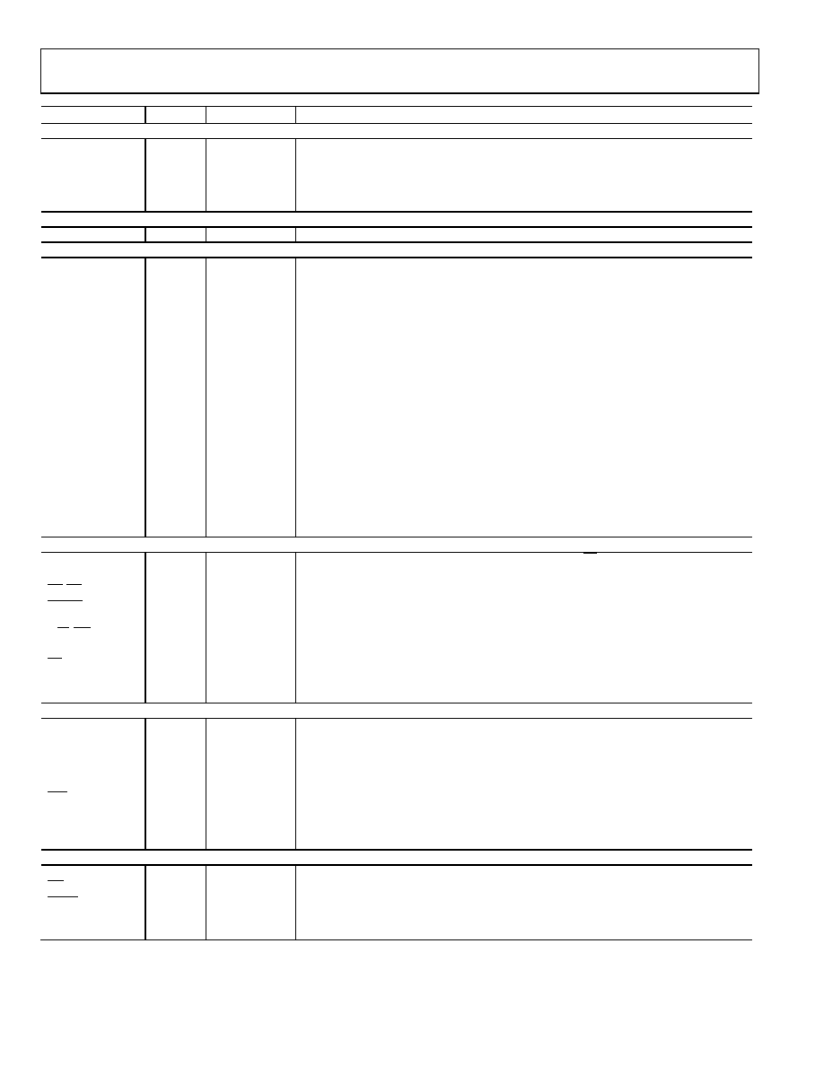
Name
Type
Pin Number
Function
DDC INPUTS
CLK
Input
A11
DDC Clock Input.
SYNC0
Input
T10
Synchronization Input 0. SYNC pins are independent of channels.
SYNC1
Input
R11
Synchronization Input 1.
SYNC2
Input
P11
Synchronization Input 2.
SYNC3
Input
T11
Synchronization Input 3.
DDC OUTPUTS
EXPC [2:0]
Output
D11, C11, B11
External VGA Gain Control Bits. GND all pins if not used.
DDC OUTPUT PORTS
PCLK
Bi-dir
T4
Parallel Output Port Clock. PCLK is bi-directional: master mode = output, slave mode = input.
PADATA[15:0]
Output
See
Parallel Output Port A Data Bus.
PACH[2:0]
Output
D8, R5, C8
Channel Indicator Output Port A.
PAIQ
Output
A8
Parallel Port A I/Q Data Indicator. Logic 1 indicates I data on data bus.
PAGAIN
Output
A9
Parallel Port A Gain Word Output Indicator. Logic 1 indicates gain word on data bus.
PAACK
Input
B8
Parallel Port A Acknowledge (Active High).
PAREQ
Output
N6
Parallel Port A Request (Active High).
PBDATA[15:0]
Output
See
Parallel Output Port B Data Bus.
PBCH[2:0]
Output
P10, P8, R8
Channel Indicator Output Port B.
PBIQ
Output
T7
Parallel Port B I/Q Data Indicator. Logic 1 indicates I data on data bus.
PBGAIN
Output
R10
Parallel Port B Gain Word Output Indicator. Logic 1 indicates gain word on data bus.
PBACK
Input
P9
Parallel Port B Acknowledge (Active High).
PBREQ
Output
N8
Parallel Port B Request (Active High)
PCDATA[15:0]
Output
See
Parallel Output Port C Data Bus.
PCCH[2:0]
Output
M5, A6, R1
Channel Indicator Output Port C.
PCIQ
Output
P1
Parallel Port C I/Q Data Indicator. Logic 1 indicates I data on data bus.
PCGAIN
Output
R2
Parallel Port C Gain word Output Indicator. Logic 1 indicates gain word on data bus.
PCACK
Input
E5
Parallel Port C Acknowledge (Active High).
PCREQ
Output
P2
Parallel Port C Request (Active High).
MICROPORT CONTROL
D[15:0]
Bi-Dir
See
Bidirectional Microport Data. This bus is three-stated when CS is high.
A[7:0]
Input
See
Microport Address Bus.
DS (RD)
Input
B4
Active Low Data Strobe, MODE = 1. Active low read strobe when MODE = 0.
DTACK (RDY)1
Output
C3
Active Low Data Acknowledge, MODE = 1. Microport status pin when MODE = 0. Terminate
to VDDIO through external 1 k pull-up resistor.
R/W (WR)
Input
C4
Read/Write Strobe, MODE = 1. Active low write strobe when MODE = 0.
MODE
Input
C2
Mode Select. Logic 0 = Intel mode, Logic 1 = Motorola mode.
CS
Input
D3
Active Low Chip Select. Logic 1 three-states the microport data bus.
CPUCLK
Input
A4
Microport CLK Input. (Input only.)
CHIPID[3:0]
Input
C1, E1, B3, B2
Chip ID Input Pins.
SERIAL PORT CONTROL
SCLK
Input
A4
Serial Clock. Should have a rise/fall time of 3ns max.
Output
C3
Serial Port Data Output. Terminate to VDDIO through external 1 k pull-up resistor.
Input
K3
Serial Port Data Input.
STFS
Input
C4
Serial Transmit Frame Sync.
SRFS
Input
B4
Serial Receive Frame Sync.
SCS
Input
D3
Serial Chip Select.
MSB_FIRST
Input
D2
Most Significant Bit_First. Selects MSB_FIRST into SDI pin, and MSB_FIRST out of SDO pin.
Logic 1 = MSB_FIRST; Logic 0 = LSB_FIRST
SMODE
Input
F1
Serial Mode Select.
MISC PINS
DNC
-------
B12, T9
Do Not Connect.
Output
E2
Interrupt Pin (Active Low). Terminate to VDDIO through external 1 k pull-up resistor.
RESET
Input
F4
Master Reset, Active Low.
EXT_FILTER
Input
D1
PLL Loop Filter (Analog Pin). Connect to VDDCORE through series 250 and 0.01 F
capacitor.
1 Pins with internal pull-up resistor of nominal 70 k.
2 Pins with internal pull-down resistor of nominal 70 k.
相关PDF资料 |
PDF描述 |
|---|---|
| AD670KNZ | IC ADC 8BIT SGNL COND 20DIP |
| AD673JNZ | IC ADC 8BIT REF/CLK/COMP 20DIP |
| AD674BJN | IC ADC 12BIT MONO 3OUT 28-DIP |
| AD676BD | IC ADC 16BIT SAMPLING 28-CDIP |
| AD677BD | IC ADC 16BIT SAMPLING 16-CDIP |
相关代理商/技术参数 |
参数描述 |
|---|---|
| AD6654BBCZ | 功能描述:IC ADC 14BIT W/6CH RSP 256CSPBGA RoHS:是 类别:集成电路 (IC) >> 数据采集 - 模数转换器 系列:- 产品培训模块:Lead (SnPb) Finish for COTS Obsolescence Mitigation Program 标准包装:250 系列:- 位数:12 采样率(每秒):1.8M 数据接口:并联 转换器数目:1 功率耗散(最大):1.82W 电压电源:模拟和数字 工作温度:-40°C ~ 85°C 安装类型:表面贴装 封装/外壳:48-LQFP 供应商设备封装:48-LQFP(7x7) 包装:管件 输入数目和类型:2 个单端,单极 |
| AD6654CBC | 功能描述:IC ADC 14BIT W/4CH RSP 256CSPBGA RoHS:否 类别:集成电路 (IC) >> 数据采集 - 模数转换器 系列:- 产品培训模块:Lead (SnPb) Finish for COTS Obsolescence Mitigation Program 标准包装:250 系列:- 位数:12 采样率(每秒):1.8M 数据接口:并联 转换器数目:1 功率耗散(最大):1.82W 电压电源:模拟和数字 工作温度:-40°C ~ 85°C 安装类型:表面贴装 封装/外壳:48-LQFP 供应商设备封装:48-LQFP(7x7) 包装:管件 输入数目和类型:2 个单端,单极 |
| AD6654CBCZ | 功能描述:IC ADC 14BIT W/4CH RSP 256CSPBGA RoHS:是 类别:集成电路 (IC) >> 数据采集 - 模数转换器 系列:- 产品培训模块:Lead (SnPb) Finish for COTS Obsolescence Mitigation Program 标准包装:250 系列:- 位数:12 采样率(每秒):1.8M 数据接口:并联 转换器数目:1 功率耗散(最大):1.82W 电压电源:模拟和数字 工作温度:-40°C ~ 85°C 安装类型:表面贴装 封装/外壳:48-LQFP 供应商设备封装:48-LQFP(7x7) 包装:管件 输入数目和类型:2 个单端,单极 |
| AD6654XBCZ | 制造商:Analog Devices 功能描述:14-BIT, 92.16 MSPS, 4 & 6-CHANNEL WIDEBAND IF TO BASE BAND R - Bulk |
| AD6655 | 制造商:AD 制造商全称:Analog Devices 功能描述:IF Diversity Receiver |
发布紧急采购,3分钟左右您将得到回复。