参数资料
| 型号: | AD6654BBC |
| 厂商: | Analog Devices Inc |
| 文件页数: | 44/88页 |
| 文件大小: | 0K |
| 描述: | IC ADC 14BIT W/6CH RSP 256CSPBGA |
| 标准包装: | 1 |
| 位数: | 14 |
| 采样率(每秒): | 92.16M |
| 数据接口: | 串行,并联 |
| 转换器数目: | 1 |
| 功率耗散(最大): | 2.5W |
| 电压电源: | 模拟和数字 |
| 工作温度: | -25°C ~ 85°C |
| 安装类型: | 表面贴装 |
| 封装/外壳: | 256-BGA,CSPBGA |
| 供应商设备封装: | 256-CSPBGA(17x17) |
| 包装: | 托盘 |
| 输入数目和类型: | 1 个差分,单极 |
第1页第2页第3页第4页第5页第6页第7页第8页第9页第10页第11页第12页第13页第14页第15页第16页第17页第18页第19页第20页第21页第22页第23页第24页第25页第26页第27页第28页第29页第30页第31页第32页第33页第34页第35页第36页第37页第38页第39页第40页第41页第42页第43页当前第44页第45页第46页第47页第48页第49页第50页第51页第52页第53页第54页第55页第56页第57页第58页第59页第60页第61页第62页第63页第64页第65页第66页第67页第68页第69页第70页第71页第72页第73页第74页第75页第76页第77页第78页第79页第80页第81页第82页第83页第84页第85页第86页第87页第88页
AD6654
Rev. 0 | Page 49 of 88
AUTOMATIC GAIN CONTROL
The AD6654 is equipped with six independent automatic gain
control (AGC) loops that directly follow the second data router
and immediately precede the parallel output ports. Each AGC
circuit has 96 dB of range. It is important that the decimating
filters of the AD6654 preceding the AGC reject unwanted
signals, so that each AGC loop is operating only on the carrier
of interest, and carriers at other frequencies do not affect the
ranging of the loop.
The AGC compresses the 22-bit complex output from the
second data router into a programmable word size of 4 to 8, 10,
12, or 16 bits. Because the small signals from the lower bits are
pushed in to higher bits by adding gain, the clipping of the
lower bits does not compromise the SNR of the signal of
interest.
The AGC maintains a constant mean power on the output
despite the level of the signal of interest, allowing operation in
environments where the dynamic range of the signal exceeds
the dynamic range of the output resolution. The output width of
the AGC is set by writing a 3-bit AGC word-length word in the
AGC control register of the individual channel’s memory map.
The AGC can be bypassed, if needed, and, when bypassed, the
24-bit complex input word remains truncated to a 16-bit value
that is output through the parallel port output. The six AGCs
available on the AD6654 are programmable through the six
channel memory maps. AGCs corresponding to individual
channels can be bypassed by writing Logic 1 to the AGC bypass
bit in the AGC control register.
Three sources of error can be introduced by the AGC function:
underflow, overflow, and modulation. Underflow is caused by
truncation of bits below the output range. Overflow is caused by
clipping errors when the output signal exceeds the output range.
Modulation error occurs when the output gain varies while
receiving data.
The desired signal level should be set based on the probability
density function of the signal, so that the errors due to under-
flow and overflow are balanced. The gain and damping values
of the loop filter should be set, so that the AGC is fast enough to
track long-term amplitude variations of the signal that might
cause excessive underflow or overflow, but slow enough to
avoid excessive loss of amplitude information due to the
modulation of the signal.
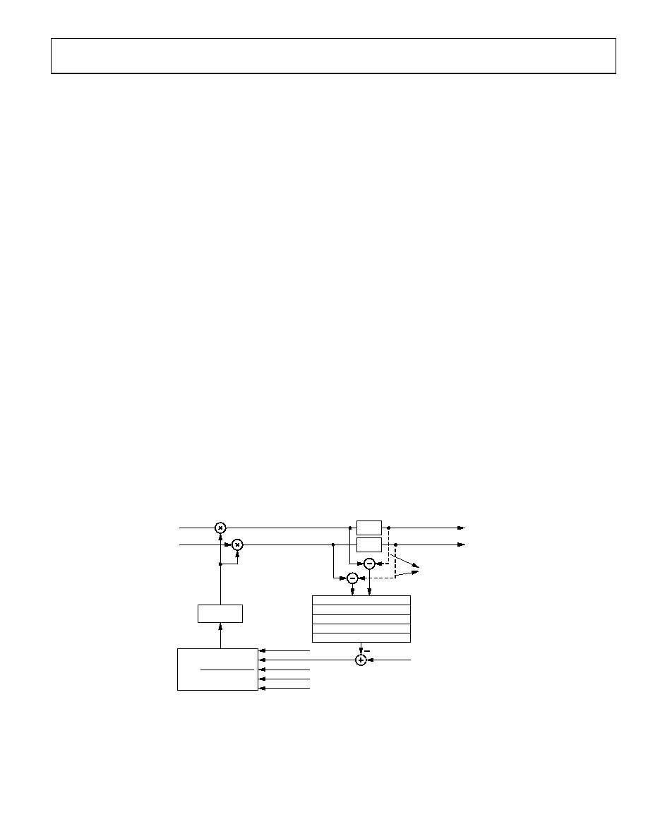
AGC LOOP
The AGC loop is implemented using a log-linear architecture. It
contains four basic operations: power calculation, error calcula-
tion, loop filtering, and gain multiplication.
The AGC can be configured to operate in either desired signal
level mode or desired clipping level mode. The mode is set by
the AGC clipping error bit of the AGC control register. The
AGC adjusts the gain of the incoming data according to how far
it is from a given desired signal level or desired clipping level,
depending on the selected mode of operation.
Two data paths to the AGC loop are provided: one before the
clipping circuitry and one after the clipping circuitry, as shown
in Figure 56. For the desired signal level mode, only the I/Q
path prior to the clipping is used. For the desired clipping level
mode, the difference of the I/Q signals from before and after the
clipping circuitry is used.
z
P
I
Q
2×
POWER OF 2
P POLE
R DESIRED
I
Q
CLIP
22
BITS
PROGRAMMABLE
BIT WIDTH
ERROR
K1 GAIN
USED ONLY FOR
DESIRED CLIPPING
LEVEL MODE
GAIN MULTIPLIER
K2 GAIN
E ERROR
THRESHOLD
SQUARE ROOT
AVERAGE 1 – 16384 SAMPLES
DECIMATE 1 – 4096 SAMPLES
log2(x)
MEAN SQUARE (I2 + Q2)
CLIP
05156-045
Kz–1
1 – (1 + ) –1 + Pz–2
G (z) =
Figure 56. Block Diagram of the AGC
相关PDF资料 |
PDF描述 |
|---|---|
| AD670KNZ | IC ADC 8BIT SGNL COND 20DIP |
| AD673JNZ | IC ADC 8BIT REF/CLK/COMP 20DIP |
| AD674BJN | IC ADC 12BIT MONO 3OUT 28-DIP |
| AD676BD | IC ADC 16BIT SAMPLING 28-CDIP |
| AD677BD | IC ADC 16BIT SAMPLING 16-CDIP |
相关代理商/技术参数 |
参数描述 |
|---|---|
| AD6654BBCZ | 功能描述:IC ADC 14BIT W/6CH RSP 256CSPBGA RoHS:是 类别:集成电路 (IC) >> 数据采集 - 模数转换器 系列:- 产品培训模块:Lead (SnPb) Finish for COTS Obsolescence Mitigation Program 标准包装:250 系列:- 位数:12 采样率(每秒):1.8M 数据接口:并联 转换器数目:1 功率耗散(最大):1.82W 电压电源:模拟和数字 工作温度:-40°C ~ 85°C 安装类型:表面贴装 封装/外壳:48-LQFP 供应商设备封装:48-LQFP(7x7) 包装:管件 输入数目和类型:2 个单端,单极 |
| AD6654CBC | 功能描述:IC ADC 14BIT W/4CH RSP 256CSPBGA RoHS:否 类别:集成电路 (IC) >> 数据采集 - 模数转换器 系列:- 产品培训模块:Lead (SnPb) Finish for COTS Obsolescence Mitigation Program 标准包装:250 系列:- 位数:12 采样率(每秒):1.8M 数据接口:并联 转换器数目:1 功率耗散(最大):1.82W 电压电源:模拟和数字 工作温度:-40°C ~ 85°C 安装类型:表面贴装 封装/外壳:48-LQFP 供应商设备封装:48-LQFP(7x7) 包装:管件 输入数目和类型:2 个单端,单极 |
| AD6654CBCZ | 功能描述:IC ADC 14BIT W/4CH RSP 256CSPBGA RoHS:是 类别:集成电路 (IC) >> 数据采集 - 模数转换器 系列:- 产品培训模块:Lead (SnPb) Finish for COTS Obsolescence Mitigation Program 标准包装:250 系列:- 位数:12 采样率(每秒):1.8M 数据接口:并联 转换器数目:1 功率耗散(最大):1.82W 电压电源:模拟和数字 工作温度:-40°C ~ 85°C 安装类型:表面贴装 封装/外壳:48-LQFP 供应商设备封装:48-LQFP(7x7) 包装:管件 输入数目和类型:2 个单端,单极 |
| AD6654XBCZ | 制造商:Analog Devices 功能描述:14-BIT, 92.16 MSPS, 4 & 6-CHANNEL WIDEBAND IF TO BASE BAND R - Bulk |
| AD6655 | 制造商:AD 制造商全称:Analog Devices 功能描述:IF Diversity Receiver |
发布紧急采购,3分钟左右您将得到回复。