参数资料
| 型号: | AD6654BBC |
| 厂商: | Analog Devices Inc |
| 文件页数: | 21/88页 |
| 文件大小: | 0K |
| 描述: | IC ADC 14BIT W/6CH RSP 256CSPBGA |
| 标准包装: | 1 |
| 位数: | 14 |
| 采样率(每秒): | 92.16M |
| 数据接口: | 串行,并联 |
| 转换器数目: | 1 |
| 功率耗散(最大): | 2.5W |
| 电压电源: | 模拟和数字 |
| 工作温度: | -25°C ~ 85°C |
| 安装类型: | 表面贴装 |
| 封装/外壳: | 256-BGA,CSPBGA |
| 供应商设备封装: | 256-CSPBGA(17x17) |
| 包装: | 托盘 |
| 输入数目和类型: | 1 个差分,单极 |
第1页第2页第3页第4页第5页第6页第7页第8页第9页第10页第11页第12页第13页第14页第15页第16页第17页第18页第19页第20页当前第21页第22页第23页第24页第25页第26页第27页第28页第29页第30页第31页第32页第33页第34页第35页第36页第37页第38页第39页第40页第41页第42页第43页第44页第45页第46页第47页第48页第49页第50页第51页第52页第53页第54页第55页第56页第57页第58页第59页第60页第61页第62页第63页第64页第65页第66页第67页第68页第69页第70页第71页第72页第73页第74页第75页第76页第77页第78页第79页第80页第81页第82页第83页第84页第85页第86页第87页第88页
AD6654
Rev. 0 | Page 28 of 88
APPLICATION INFORMATION
ADC CONFIGURATION NOTES
Encoding the AD6654 ADC
The AD6654 encode signal must be a high quality, extremely
low phase noise source to prevent degradation of performance.
Maintaining 14-bit accuracy places a premium on encode clock
phase noise. SNR performance can easily degrade by 3 dB to
4 dB with 70 MHz analog input signals when using a high jitter
clock source. See the AN-501, Aperture Uncertainty and ADC
System Performance Application Note
, for details.
For optimum performance, the AD6654 ADC front end must
be clocked differentially. The encode signals are usually ac-
coupled into the ENC+ and ENC pins via a transformer or
capacitors. The ENCODE pins are biased internally and require
no additional bias.
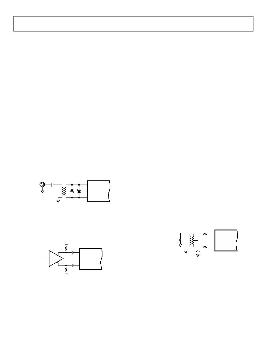
Figure 37 shows one preferred method for clocking the
AD6654. The clock source (low jitter) is converted from single-
ended to differential using an RF transformer. The back-to-back
Schottky diodes across the secondary of the transformer limit
clock excursions into the AD6654 to approximately 0.8 V p-p
differential. This helps prevent the large voltage swings of the
clock from feeding through to other portions of the AD6654,
and limits the noise presented to the encode inputs.
ENC+
ENC–
0.1
F
T1-4T
HSMS2812
DIODES
AD6654
CLOCK
SOURCE
05156-027
Figure 37. Crystal Clock Oscillator-Differential Encode
If a low jitter clock is available, another option is to ac-couple a
differential ECL/PECL signal to the encode input pins as shown
in Figure 38. A device that offers excellent jitter performance is
the MC100EL16 (or same family) from ON Semiconductor.
ENC+
ENC–
AD6654
VT
0.1
F
0.1
F
ECL/
PECL
05156-028
Figure 38. Differential ECL for Encode
Driving the Analog Inputs
As with most high speed, high dynamic range ADCs, the analog
input to the AD6654 front end is differential. Differential inputs
improve on-chip performance, because signals are processed
through attenuation and gain stages. Most of the improvement
is a result of differential analog stages having high rejection of
even-order harmonics.
There are also benefits at the PCB level. First, differential inputs
have high common-mode rejection to stray signals such as
ground and power noise. Second, they provide good rejection to
common-mode signals such as local oscillator feed-through.
The AD6654 analog input pins, AIN+ and AIN, are centered
at 2.4 V, and the signal at each input should swing ±0.55 V
around this voltage. Because AIN+ and AIN are 180° out of
phase, the full-scale differential analog input signal is 2.2 V p-p.
Each analog input connects through a 500 resistor to the
2.4 V bias voltage and to the input of a differential buffer, as
shown in Figure 36. The resistor network on the input properly
biases the followers for maximum linearity and range.
Therefore, the analog source driving the AD6654 should be
ac-coupled to the input pins. Because the differential input
impedance of the AD6654 is 1 k, the analog input power
requirement is only 2 dBm, simplifying the driver amplifier in
many cases. To take full advantage of this high input
impedance, a 20:1 transformer is required. This is a large ratio
that could result in unsatisfactory performance. In this case, a
lower step-up ratio could be used. The recommended method
for driving the analog input of the AD6654 is to use a 4:1
impedance ratio RF transformer.
For example, if RT is set to 60.4 and RS is set to 25 , along
with a 4:1 impedance ratio transformer, the input matches to a
50 source with a full-scale drive of 4.8 dBm. Series resistors
(RS) on the secondary side of the transformer should be used to
isolate the transformer from A/D. This limits the amount of
dynamic current from the A/D flowing back into the secondary
of the transformer. The 50 impedance matching can also be
incorporated on the secondary side of the transformer, as
shown in the evaluation board schematic.
AIN–
AIN+
ADT4-1WT
AD6654
ANALOG INPUT
SIGNAL
0.1
F
RT
RS
05156-029
Figure 39. Transformer-Coupled Analog Input Circuit
In applications where dc-coupling, or additional gain is
required, use a differential output op amp from Analog Devices,
Inc., such as AD8351, to drive the AD6654 (Figure 40). The
AD8351 op amp can be driven differentially, or configured to
provide single-ended-to-differential conversion.
相关PDF资料 |
PDF描述 |
|---|---|
| AD670KNZ | IC ADC 8BIT SGNL COND 20DIP |
| AD673JNZ | IC ADC 8BIT REF/CLK/COMP 20DIP |
| AD674BJN | IC ADC 12BIT MONO 3OUT 28-DIP |
| AD676BD | IC ADC 16BIT SAMPLING 28-CDIP |
| AD677BD | IC ADC 16BIT SAMPLING 16-CDIP |
相关代理商/技术参数 |
参数描述 |
|---|---|
| AD6654BBCZ | 功能描述:IC ADC 14BIT W/6CH RSP 256CSPBGA RoHS:是 类别:集成电路 (IC) >> 数据采集 - 模数转换器 系列:- 产品培训模块:Lead (SnPb) Finish for COTS Obsolescence Mitigation Program 标准包装:250 系列:- 位数:12 采样率(每秒):1.8M 数据接口:并联 转换器数目:1 功率耗散(最大):1.82W 电压电源:模拟和数字 工作温度:-40°C ~ 85°C 安装类型:表面贴装 封装/外壳:48-LQFP 供应商设备封装:48-LQFP(7x7) 包装:管件 输入数目和类型:2 个单端,单极 |
| AD6654CBC | 功能描述:IC ADC 14BIT W/4CH RSP 256CSPBGA RoHS:否 类别:集成电路 (IC) >> 数据采集 - 模数转换器 系列:- 产品培训模块:Lead (SnPb) Finish for COTS Obsolescence Mitigation Program 标准包装:250 系列:- 位数:12 采样率(每秒):1.8M 数据接口:并联 转换器数目:1 功率耗散(最大):1.82W 电压电源:模拟和数字 工作温度:-40°C ~ 85°C 安装类型:表面贴装 封装/外壳:48-LQFP 供应商设备封装:48-LQFP(7x7) 包装:管件 输入数目和类型:2 个单端,单极 |
| AD6654CBCZ | 功能描述:IC ADC 14BIT W/4CH RSP 256CSPBGA RoHS:是 类别:集成电路 (IC) >> 数据采集 - 模数转换器 系列:- 产品培训模块:Lead (SnPb) Finish for COTS Obsolescence Mitigation Program 标准包装:250 系列:- 位数:12 采样率(每秒):1.8M 数据接口:并联 转换器数目:1 功率耗散(最大):1.82W 电压电源:模拟和数字 工作温度:-40°C ~ 85°C 安装类型:表面贴装 封装/外壳:48-LQFP 供应商设备封装:48-LQFP(7x7) 包装:管件 输入数目和类型:2 个单端,单极 |
| AD6654XBCZ | 制造商:Analog Devices 功能描述:14-BIT, 92.16 MSPS, 4 & 6-CHANNEL WIDEBAND IF TO BASE BAND R - Bulk |
| AD6655 | 制造商:AD 制造商全称:Analog Devices 功能描述:IF Diversity Receiver |
发布紧急采购,3分钟左右您将得到回复。