参数资料
| 型号: | AD6654BBC |
| 厂商: | Analog Devices Inc |
| 文件页数: | 77/88页 |
| 文件大小: | 0K |
| 描述: | IC ADC 14BIT W/6CH RSP 256CSPBGA |
| 标准包装: | 1 |
| 位数: | 14 |
| 采样率(每秒): | 92.16M |
| 数据接口: | 串行,并联 |
| 转换器数目: | 1 |
| 功率耗散(最大): | 2.5W |
| 电压电源: | 模拟和数字 |
| 工作温度: | -25°C ~ 85°C |
| 安装类型: | 表面贴装 |
| 封装/外壳: | 256-BGA,CSPBGA |
| 供应商设备封装: | 256-CSPBGA(17x17) |
| 包装: | 托盘 |
| 输入数目和类型: | 1 个差分,单极 |
第1页第2页第3页第4页第5页第6页第7页第8页第9页第10页第11页第12页第13页第14页第15页第16页第17页第18页第19页第20页第21页第22页第23页第24页第25页第26页第27页第28页第29页第30页第31页第32页第33页第34页第35页第36页第37页第38页第39页第40页第41页第42页第43页第44页第45页第46页第47页第48页第49页第50页第51页第52页第53页第54页第55页第56页第57页第58页第59页第60页第61页第62页第63页第64页第65页第66页第67页第68页第69页第70页第71页第72页第73页第74页第75页第76页当前第77页第78页第79页第80页第81页第82页第83页第84页第85页第86页第87页第88页
AD6654
Rev. 0 | Page 79 of 88
CIC Decimation <4:0>
This 5-bit word specifies the CIC filter decimation value
minus 1. A value of 0x00 is a decimation of 1 (bypass), and
0x1F is a decimation of 32. Writing a value of 0 in this register
bypasses CIC filtering, but does not bypass the CIC scaling
operation.
CIC Scale Factor <4:0>
This 5-bit word specifies the CIC filter scale factor used to
compensate for the gain provided by the CIC filter. The
recommended value is given by the following equation:
5
))
(
log
5
(
2
×
=
CIC
M
ceil
Register
Scale
CIC
where:
MCIC
is the decimation rate of the CIC (one more than the value
in the CIC decimation register).
ceil
operation gives the closest integer greater than or equal to
the argument.
The valid range for this register is decimal 0 to 20.
FIR-HB Control <3:0>
<3>: FIR1 Enable Bit. When this bit is set, the FIR1 fixed
coefficient filter is enabled. When cleared, FIR1 is bypassed.
<2>: HB1 Enable Bit. When this bit is set, the HB1 half-band
filter is enabled. When cleared, HB1 is bypassed.
<1>: FIR2 Enable Bit. When this bit is set, the FIR2 fixed
coefficient filter is enabled. When cleared, FIR2 is bypassed.
<0>: HB2 Enable Bit. When this bit is set, the HB2 half-band
filter is enabled. When cleared, HB2 is bypassed.
MRCF Control Register <12:0>
<12:10>: MRCF Data Select Bits. These bits are used to select
the input source for the MRCF filter. Each MRCF filter can be
driven by output from the HB2 filter of any channel independ-
ently. Table 35 shows the selections available.
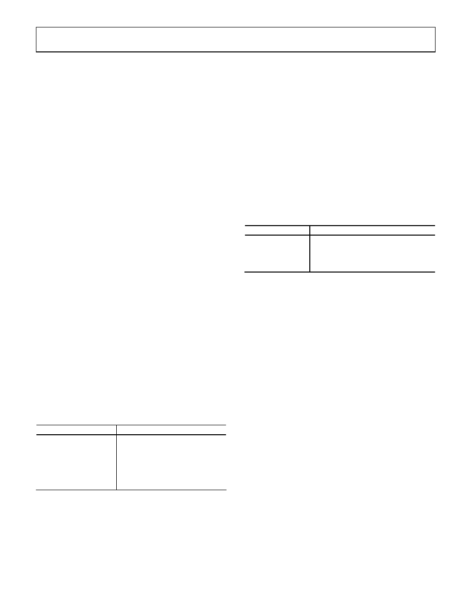
Table 35. MRCF Data Select Bits
MRCF Data Select<2:0>
MRCF Input Source
000
MRCF input taken from Channel 0
001
MRCF input taken from Channel 1
010
MRCF input taken from Channel 2
011
MRCF input taken from Channel 3
1x0
MRCF input taken from Channel 4
1x1
MRCF input taken from Channel 5
<9>: Interpolating Half-Band Enable Bit. When this bit is set,
the interpolating half-band filter, driven by the output of the
CRCF block, is enabled. When cleared, the interpolating half-
band filter is bypassed, and its output is the same as its input.
The interpolating half-band filter doubles the data rate.
<8>: This bit is open.
<7>: Half-Rate Bit. When this bit is set, the MRCF filter
operates using half the PLL clock rate. This is used for power
savings when there is sufficient time to complete MRCF
filtering using only half the PLL clock rate. When this bit is
cleared, the MRCF filter operates at the full PLL clock rate. See
the Mono-Rate RAM Coefficient Filter (MRCF) section.
<6:4>: MRCF Number of Taps Bits. This 3-bit word should be
written with one less than the number of taps that are calculated
by the MRCF filter. The filter length is given by the decimal
value of this register plus 1. A value of 0 represents a 1-tap filter
and maximum value of 7 represents an 8-tap filter.
<3:2>: MRCF Scale Factor Bits. The output of the MRCF filter is
scaled according to the value of these bits. Table 36 describes
the attenuation corresponding to each setting.
Table 36. MRCF Scale Factor
MRCF Scale<1:0>
Scale Factor
00
18.06 dB attenuation (left-shift 3 bits)
01
12.04 dB attenuation (left-shift 2 bits)
10
6.02 dB attenuation (left-shift 1 bit)
11
No scaling (0 dB)
<1>: This bit is open.
<0>: MRCF Bypass Bit. When this bit is set, the MRCF filter is
bypassed and, therefore, the output of the MRCF is the same as
its input. When this bit is cleared, the MRCF has normal
operation as programmed by its control register.
MRCF COEFFICIENT MEMORY
The MRCF coefficient memory consists of eight coefficients,
each six bits wide. The memory extends from Address 0x80 to
Address 0x87. The coefficients should be written in twos
complement format.
DRCF Control Register <11:0>
<11>: DRCF Bypass Bit. When this bit is set, the DRCF filter is
bypassed and, therefore, its output is the same as its input.
When this bit is cleared, the DRCF has normal operation as
programmed by the rest of this control register.
<10>: Symmetry Bit. When this bit is set, it indicates that the
DRCF is implementing a symmetrical filter and only half the
impulse response needs to be written into the DRCF coefficient
RAM. When this bit is cleared, the filter is asymmetrical and
complete impulse response of the filter should be written to the
coefficient RAM. When this filter is symmetrical, it can imple-
ment up to 128 filter taps.
<9:8>: DRCF Multiply Accumulate Scale Bits. The output of the
DRCF filter is scaled according to the value of these bits.
Table 37 lists the attenuation corresponding to each setting.
相关PDF资料 |
PDF描述 |
|---|---|
| AD670KNZ | IC ADC 8BIT SGNL COND 20DIP |
| AD673JNZ | IC ADC 8BIT REF/CLK/COMP 20DIP |
| AD674BJN | IC ADC 12BIT MONO 3OUT 28-DIP |
| AD676BD | IC ADC 16BIT SAMPLING 28-CDIP |
| AD677BD | IC ADC 16BIT SAMPLING 16-CDIP |
相关代理商/技术参数 |
参数描述 |
|---|---|
| AD6654BBCZ | 功能描述:IC ADC 14BIT W/6CH RSP 256CSPBGA RoHS:是 类别:集成电路 (IC) >> 数据采集 - 模数转换器 系列:- 产品培训模块:Lead (SnPb) Finish for COTS Obsolescence Mitigation Program 标准包装:250 系列:- 位数:12 采样率(每秒):1.8M 数据接口:并联 转换器数目:1 功率耗散(最大):1.82W 电压电源:模拟和数字 工作温度:-40°C ~ 85°C 安装类型:表面贴装 封装/外壳:48-LQFP 供应商设备封装:48-LQFP(7x7) 包装:管件 输入数目和类型:2 个单端,单极 |
| AD6654CBC | 功能描述:IC ADC 14BIT W/4CH RSP 256CSPBGA RoHS:否 类别:集成电路 (IC) >> 数据采集 - 模数转换器 系列:- 产品培训模块:Lead (SnPb) Finish for COTS Obsolescence Mitigation Program 标准包装:250 系列:- 位数:12 采样率(每秒):1.8M 数据接口:并联 转换器数目:1 功率耗散(最大):1.82W 电压电源:模拟和数字 工作温度:-40°C ~ 85°C 安装类型:表面贴装 封装/外壳:48-LQFP 供应商设备封装:48-LQFP(7x7) 包装:管件 输入数目和类型:2 个单端,单极 |
| AD6654CBCZ | 功能描述:IC ADC 14BIT W/4CH RSP 256CSPBGA RoHS:是 类别:集成电路 (IC) >> 数据采集 - 模数转换器 系列:- 产品培训模块:Lead (SnPb) Finish for COTS Obsolescence Mitigation Program 标准包装:250 系列:- 位数:12 采样率(每秒):1.8M 数据接口:并联 转换器数目:1 功率耗散(最大):1.82W 电压电源:模拟和数字 工作温度:-40°C ~ 85°C 安装类型:表面贴装 封装/外壳:48-LQFP 供应商设备封装:48-LQFP(7x7) 包装:管件 输入数目和类型:2 个单端,单极 |
| AD6654XBCZ | 制造商:Analog Devices 功能描述:14-BIT, 92.16 MSPS, 4 & 6-CHANNEL WIDEBAND IF TO BASE BAND R - Bulk |
| AD6655 | 制造商:AD 制造商全称:Analog Devices 功能描述:IF Diversity Receiver |
发布紧急采购,3分钟左右您将得到回复。