参数资料
| 型号: | AD6654BBC |
| 厂商: | Analog Devices Inc |
| 文件页数: | 50/88页 |
| 文件大小: | 0K |
| 描述: | IC ADC 14BIT W/6CH RSP 256CSPBGA |
| 标准包装: | 1 |
| 位数: | 14 |
| 采样率(每秒): | 92.16M |
| 数据接口: | 串行,并联 |
| 转换器数目: | 1 |
| 功率耗散(最大): | 2.5W |
| 电压电源: | 模拟和数字 |
| 工作温度: | -25°C ~ 85°C |
| 安装类型: | 表面贴装 |
| 封装/外壳: | 256-BGA,CSPBGA |
| 供应商设备封装: | 256-CSPBGA(17x17) |
| 包装: | 托盘 |
| 输入数目和类型: | 1 个差分,单极 |
第1页第2页第3页第4页第5页第6页第7页第8页第9页第10页第11页第12页第13页第14页第15页第16页第17页第18页第19页第20页第21页第22页第23页第24页第25页第26页第27页第28页第29页第30页第31页第32页第33页第34页第35页第36页第37页第38页第39页第40页第41页第42页第43页第44页第45页第46页第47页第48页第49页当前第50页第51页第52页第53页第54页第55页第56页第57页第58页第59页第60页第61页第62页第63页第64页第65页第66页第67页第68页第69页第70页第71页第72页第73页第74页第75页第76页第77页第78页第79页第80页第81页第82页第83页第84页第85页第86页第87页第88页
AD6654
Rev. 0 | Page 54 of 88
PCLK
tDPREQ
PxREQ
PxACK
tDPP
Px [15:0]
I[15:0]
Q[15:0]
PxIQ
tDPIQ
PxCH [2:0]
PxCH [2:0] = CHANNEL #
tDPCH
0000 +
GAIN [11:0]
PxGAIN
tDPGAIN
05156-047
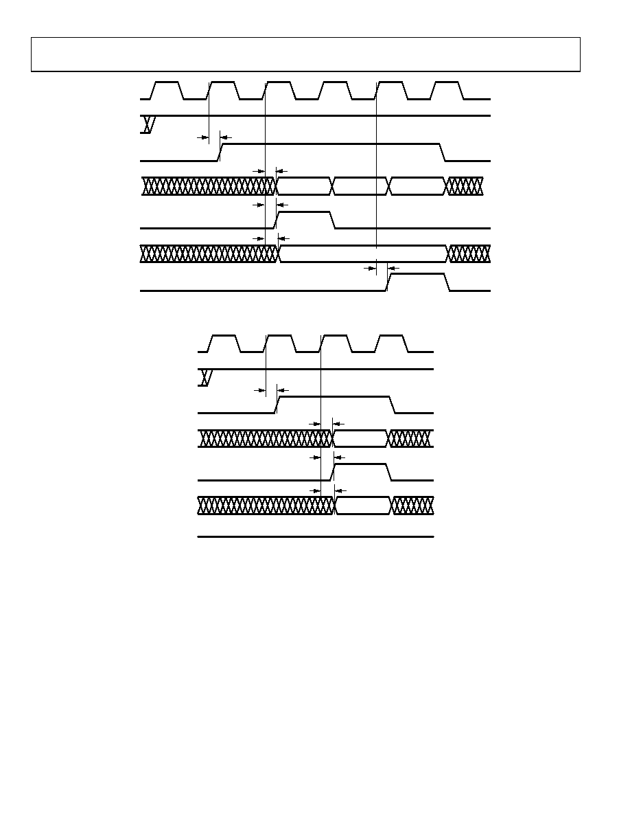
Figure 58. Interleaved I/Q Mode with an AGC Gain Word
PxCH [2:0]
PCLK
tDPREQ
PxREQ
PxACK
tDPP
Px [15:0]
I [15:8]
Q [15:8]
PxIQ
tDPIQ
PxCH [2:0] =
AGC NO.
tDPCH
PxGAIN
LOGIC LOW 0
05156-048
Figure 59. Parallel I/Q Mode Without an AGC Gain Word
When an output data sample is available for output from an
AGC, the parallel port initiates the transfer by pulling the
PxREQ signal high. In response, the processor receiving the
data needs to pull the PxACK signal high, acknowledging that it
is ready to receive the signal. In Figure 59, the PxACK is already
pulled high and, therefore, the 8-bit I data and 8-bit Q data are
simultaneously output on the data bus on the next PCLK rising
edge after PxREQ is driven logic high. The PxIQ signal also
goes high to indicate that I/Q data is available on the data bus.
When I/Q data is being output, the channel indicator pins
PxCH[2:0] indicate the data source (AGC number).
Figure 59 is the timing diagram for parallel I/Q mode with the
AGC gain word disabled. Figure 60 is a similar timing diagram
with the AGC gain word enabled. In the PCLK cycle after the
I/Q data, the AGC gain word is output on the data bus, and the
PxGAIN signal is pulled high to indicate that the gain word is
available on the parallel port. During this PCLK cycle, the PxIQ
signal is pulled low to indicate that I/Q data is not available on
the data bus. Therefore, in parallel I/Q mode, a minimum of
two PCLK cycles is required to output one sample of output
data on the parallel port without and with the AGC gain word,
respectively.
The order of data output is dependent on when data arrives at
the port, which is a function of total decimation rate, DRCF/
CRCF decimation phase, and start hold-off values. Priority
order from highest to lowest is, AGC0, AGC1, AGC2, AGC3,
AGC4, and AGC5 for both parallel I/Q and interleaved modes
of output.
相关PDF资料 |
PDF描述 |
|---|---|
| AD670KNZ | IC ADC 8BIT SGNL COND 20DIP |
| AD673JNZ | IC ADC 8BIT REF/CLK/COMP 20DIP |
| AD674BJN | IC ADC 12BIT MONO 3OUT 28-DIP |
| AD676BD | IC ADC 16BIT SAMPLING 28-CDIP |
| AD677BD | IC ADC 16BIT SAMPLING 16-CDIP |
相关代理商/技术参数 |
参数描述 |
|---|---|
| AD6654BBCZ | 功能描述:IC ADC 14BIT W/6CH RSP 256CSPBGA RoHS:是 类别:集成电路 (IC) >> 数据采集 - 模数转换器 系列:- 产品培训模块:Lead (SnPb) Finish for COTS Obsolescence Mitigation Program 标准包装:250 系列:- 位数:12 采样率(每秒):1.8M 数据接口:并联 转换器数目:1 功率耗散(最大):1.82W 电压电源:模拟和数字 工作温度:-40°C ~ 85°C 安装类型:表面贴装 封装/外壳:48-LQFP 供应商设备封装:48-LQFP(7x7) 包装:管件 输入数目和类型:2 个单端,单极 |
| AD6654CBC | 功能描述:IC ADC 14BIT W/4CH RSP 256CSPBGA RoHS:否 类别:集成电路 (IC) >> 数据采集 - 模数转换器 系列:- 产品培训模块:Lead (SnPb) Finish for COTS Obsolescence Mitigation Program 标准包装:250 系列:- 位数:12 采样率(每秒):1.8M 数据接口:并联 转换器数目:1 功率耗散(最大):1.82W 电压电源:模拟和数字 工作温度:-40°C ~ 85°C 安装类型:表面贴装 封装/外壳:48-LQFP 供应商设备封装:48-LQFP(7x7) 包装:管件 输入数目和类型:2 个单端,单极 |
| AD6654CBCZ | 功能描述:IC ADC 14BIT W/4CH RSP 256CSPBGA RoHS:是 类别:集成电路 (IC) >> 数据采集 - 模数转换器 系列:- 产品培训模块:Lead (SnPb) Finish for COTS Obsolescence Mitigation Program 标准包装:250 系列:- 位数:12 采样率(每秒):1.8M 数据接口:并联 转换器数目:1 功率耗散(最大):1.82W 电压电源:模拟和数字 工作温度:-40°C ~ 85°C 安装类型:表面贴装 封装/外壳:48-LQFP 供应商设备封装:48-LQFP(7x7) 包装:管件 输入数目和类型:2 个单端,单极 |
| AD6654XBCZ | 制造商:Analog Devices 功能描述:14-BIT, 92.16 MSPS, 4 & 6-CHANNEL WIDEBAND IF TO BASE BAND R - Bulk |
| AD6655 | 制造商:AD 制造商全称:Analog Devices 功能描述:IF Diversity Receiver |
发布紧急采购,3分钟左右您将得到回复。